How to design an overvoltage protection circuit?
tags: Circuit design 1024 Programmer's Day How to design an overvoltage protection circuit? How to choose TVS tube? Power protection circuit design
table of Contents
1. Save money and worry about TVS tube
1.3, the actual circuit application
2. Reliable and efficient circuit
The function of the overvoltage protection circuit is to limit the output voltage to a safe value range if the internal voltage regulation loop of the switching power supply fails or the output voltage exceeds the design threshold due to improper operation by the user, in order to protect the subsequent electrical equipment from damage .
This blog post will introduce how to quickly design an overvoltage protection circuit from two methods of saving money and worrying TVS tube and reliable and efficient circuit design.
1. Save money and worry about TVS tube
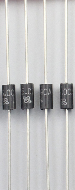
TVS (Transient Voltage Suppressors), that is, transient voltage suppressor, also known as avalanche breakdown diode, is a high-efficiency protection device in the form of a diode.
1.1, TVS tube characteristics
TVS tube is divided into one-way and two-way, one-way TVS tube is generally used in DC power supply circuits, and two-way TVS tube is used in circuits with alternating voltage.
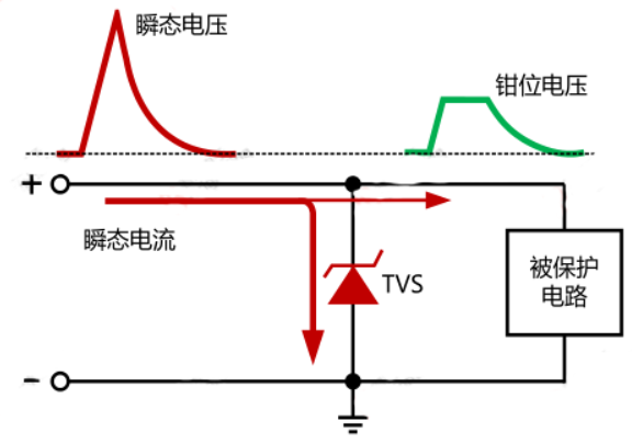
For example, when a one-way TVS tube is applied to a DC circuit, as shown in the figure below. When the circuit works normally, the TVS is in the cut-off state (high impedance state), which does not affect the normal operation of the circuit.When an abnormal overvoltage occurs in the circuit and the TVS (avalanche) breakdown voltage is reached, the TVS rapidly changes from a high resistance state to a low resistance state, and discharges the instantaneous overcurrent caused by the abnormal overvoltage to the ground, and at the same time clamps the abnormal overvoltage to the ground. A lower level to protect the subsequent circuit from abnormal overvoltage damage.When the abnormal overvoltage disappears, the resistance of the TVS returns to a high-impedance state.
There are several important parameters for selecting TVS tubes:
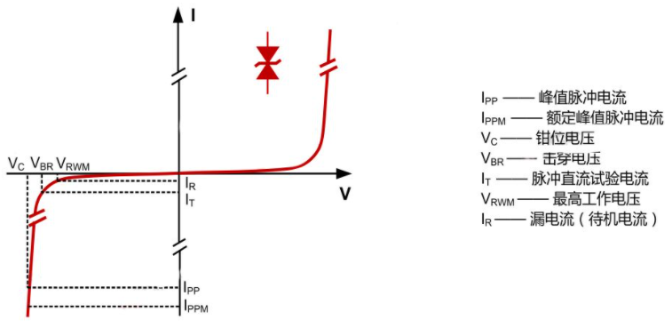
(1) Vrwm cut-off voltage
The highest working voltage of TVS,The highest operating peak voltage or DC peak voltage that can be continuously applied without causing degradation or damage to the TVS.For AC voltage, it is expressed by the effective value of the highest working voltage. Under Vrwm, TVS thinks it is not working, that is, it is not conducting. The maximum working voltage of the circuit design must be less than Vrwm, otherwise it will cause the TVS to operate and cause the circuit to be abnormal.
(2) IR leakage current
Leakage current, also called standby current.The maximum current that flows through the TVS under the specified temperature and maximum operating voltage conditions.The leakage current of TVS is generally measured under the cut-off voltage. For a certain type of TVS, IR should be within the specified value range. The voltage value applied to both ends of the TVS is Vrwm, and the current value read from the ammeter is the leakage current IR of the TVS. For TVS of the same power and voltage, when Vrwm≤10V, the leakage current of the two-way TVS is twice that of the one-way TVS. For some analog ports,Leakage current will affect the sampling value of AD, so the smaller the leakage current of TVS, the better。
(3) VBR breakdown voltage
Breakdown voltage refers to the voltage across the TVS measured on the V-I characteristic curve under the specified pulse DC current It or the current conditions close to the avalanche. The test current It is generally about 10mA, and the applied current should not exceed 400ms to avoid damage to the device. VBR MIN and VBR MAX are a deviation of the breakdown voltage of the TVS. Generally, the deviation of the TVS is ±5%. When measuring, VBR falling between VBR MIN and VBR MAX is regarded as a qualified product.
(4) IPP peak pulse current, VC clamp voltage
Peak pulse current, given the peak value of the pulse current waveform. TVS generally uses 10/1000μs current waveform. Clamping voltage, the peak voltage measured across the TVS when the peak pulse current I PP of the specified waveform is applied. IPP and VC are parameters that measure the ability of TVS to resist surge pulse current and limit voltage in circuit protection. These two parameters are related to each other. For the clamping characteristics of TVS in the lightning protection circuit, you can refer to the VC parameter. For the same type of TVS, the larger the IPP, the stronger the ability to withstand the impact of pulse current. If the VC under the same IPP is the smaller, the better the clamping characteristics of the TVS.
(5) Junction capacitance Cj
Junction capacitance is the parasitic capacitance in TVS, and it is important to pay attention to high-speed IO port protection.Excessive junction capacitance may affect the quality of the signal.
1.2 Selection of TVS tube
There are three main points to pay attention to when choosing TVS tube:
- Proper voltage can protect the subsequent circuit;
- The junction capacitance of the introduced TVS cannot affect the circuit;
- The TVS has sufficient power margin to meet the test standards and cannot be hung before the fuse.
The selection process can be carried out according to the following steps:
- Select the highest working voltage Vrmw of TVS;
- Select TVS clamp voltage VC;
- Select the power of TVS;
- Evaluate the influence of leakage current Ir;
- Evaluate the effect of junction capacitance.
The specific instructions are as follows:
(1) Select the highest working voltage Vrmw of TVS
In the normal working condition of the circuit, the TVS should not work, that is, in the cut-off state, so the cut-off voltage of the TVS should be greater than the highest working voltage of the protected circuit. In this way, it can be ensured that the TVS will not affect the circuit operation under the normal operation of the circuit. However, the TVS working voltage also determines the TVS clamping voltage. When the cut-off voltage is greater than the normal working voltage of the line, the TVS working voltage cannot be selected too high. If it is too high, the clamping voltage will be higher. Therefore, when choosing Vrwm, it is necessary to comprehensively consider the working voltage of the protected circuit and the endurance of the subsequent circuit. Vrwm is required to be greater than the operating voltage, otherwise the operating voltage greater than Vrwm will cause the TVS reverse leakage current to increase, close to conduction, or avalanche breakdown, affecting normal circuit operation.
Vrwm can refer to the following formula:
Vrwm≈1.1~1.2*VCC (where VCC is the highest working voltage of the circuit)(2) Select TVS clamp voltage VC
The clamping voltage of TVS should be less than the maximum tolerable transient safety voltage of the subsequent protected circuit. VC is proportional to the avalanche breakdown voltage and IPP of the TVS. For TVS of the same power level, the higher the breakdown voltage, the higher the VC. The maximum clamping voltage VC of the selected TVS cannot be greater than the maximum voltage that the protected circuit can withstand. Otherwise, the circuit will be damaged when the TVS clamps on the VC.
Vc can refer to the following formula:
VC<Vmax (where Vmax is the highest voltage that the circuit can withstand)(3) Select TVS power Pppm (or Ipp)
The rated transient power of TVS products should be greater than the maximum transient surge power that may appear in the circuit. Theoretically, the greater the power of the TVS, the better, and it can withstand more impact energy and times, but the higher the power, the more the TVS package is. The larger the price, the higher the price, so the power of the TVS can meet the requirements. For TVS of different power levels, the V C value of the TVS of the same voltage specification is the same, but the I PP is different. Therefore, Pppm is directly proportional to Ippm. The greater the Ippm, the greater the Pppm. For a certain circuit, there is a corresponding test requirement. If the maximum test current in the actual circuit is Iactual, then Iactual can be estimated as:
Iactual=Uactual/Ri (Uactual is the test voltage, Ri is the test internal resistance)TVS must pass the test, so the actual circuit requires that the minimum power P actual of the TVS under the 10/1000μs waveform is: ------- where di/dt is the waveform conversion coefficient, if the actual test waveform is other waveforms, such as 8/ 20μs waveform, it is recommended to take di/dt. If the test waveform is 10/1000μs, take it. In actual selection, TVS should have a certain margin, and TVS power PPMP selection should follow Pppm>Pactual.
(4) Evaluate the impact based on the junction capacitance and leakage current of the selected TVS
If TVS is used in high-speed IO port protection, analog signal sampling, and low-power devices, the effects of junction capacitance and leakage current need to be considered. The smaller the two parameters, the better.
Selection example
For example: the normal operating voltage VCC of the circuit is 24V, the highest operating voltage Vmax is 26V, the highest transient voltage that the subsequent circuit can withstand is 50V, the test waveform of the experiment is 8/20μs waveform, the test voltage is 500V, and the internal resistance of the power supply is tested. The total static resistance of PPTC is 2Ω. Select the appropriate TVS based on the above information.
(1) Select the highest working voltage of TVS
Vrmw≈1.1~1.2*VCC=26~28V
(2) Choose to choose TVS clamp voltage
VC<Vmax=50V
(3) Calculate the actual test waveform power:
Pact=50*(500/3)*1/2=4166W
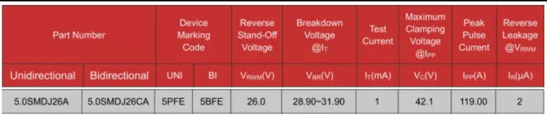
According to the calculation result, the TVS 5.0SMDJ26A can be selected. Since this TVS is used in the power port, the junction capacitance and leakage current can be selected according to the actual circuit.
1.3, the actual circuit application
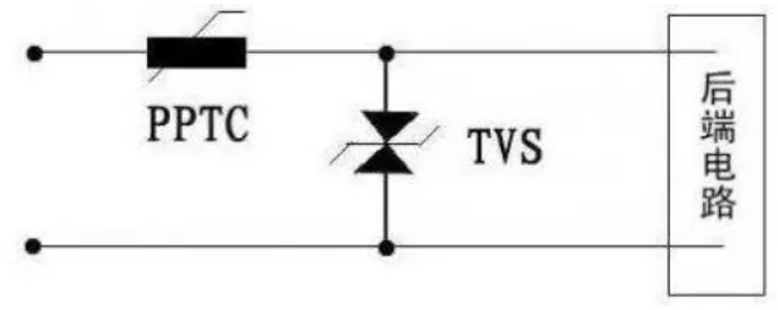
When the working voltage of the port of the device exceeds the maximum breakdown voltage (VBR MAX) of the TVS, the TVS can be regarded as a low-impedance resistor. The current flowing through is very large and the resistor keeps heating up. If no other measures are taken, the TVS is very fast. It will hang up, and the failed TVS will most likely become an open circuit, and the subsequent circuit will still be unprotected.Therefore, it is best to add a fuse in front of the TVS. Before the TVS hangs up, the fuse will fail and break to protect the TVS and the subsequent circuit. If it is replaced with a self-recoverable fuse, the normal operation can be restored by itself after troubleshooting.
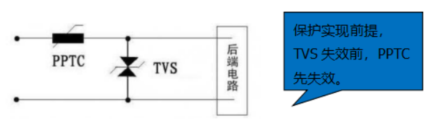
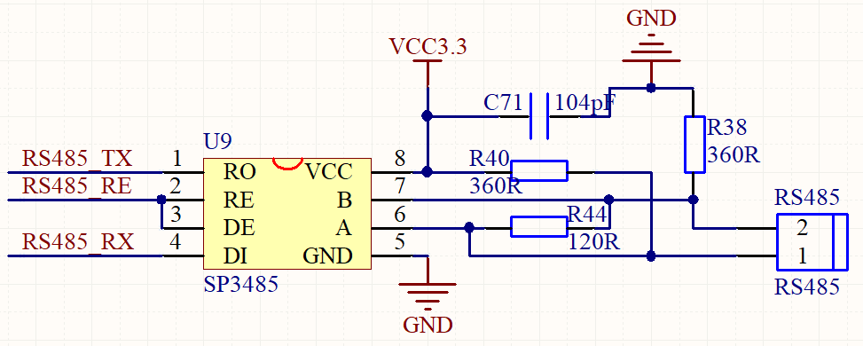
The following figure shows the RS485 overvoltage protection circuit. The working voltage of the RS485 chip is generally 5V, and the limit voltage that it can withstand is generally 12V. Usually the working voltage of the equipment is generally 12V or 24V. If the 24V power supply voltage is connected to the RS485A-B line by mistake and there is no overvoltage protection, there is a high probability that the RS485 chip will be physically damaged.TVS tube is specially used for instantaneous overvoltage protection, Unable to cope with long-term overvoltage, less than 0.5STVS will burn out due to overheating, and the subsequent circuit will lose its protection.
If a self-recovering PTC is added in front of the TVS, and the tripping time of the PTC is short enough, and the clamping voltage Vc of the TVS <the highest working voltage VCC of the circuit, the PTC trips before the TVS burns, and the protection of the subsequent circuit can be realized. To
The calculation process of the TVS tube and self-recoverable PPTC is as follows:
(1) Preconditions for realization of protection
When the applied voltage reaches the breakdown voltage of the TVS, the TVS starts to turn on, the impedance becomes lower, and the current flowing through it increases. As the current continues to increase, the impedance of the PPTC continues to increase, and it continues to heat up. Finally, the PPTC becomes an open circuit and fails, and the entire subsequent circuit is protected. Therefore, to realize circuit protection, two prerequisites are required:
- The power of TVS is large enough to persist until PPTC is disconnected;
- The action time of PPTC should be small enough to move before TVS fails.
(2) PPTC selection
When used for overvoltage protection, the selection of PPTC needs to meet the following conditions:
- Continuous current Ihold>The maximum working current of the circuit Iwork;
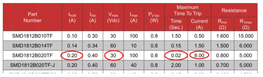
- The shorter the maximum action time Trip, the better, such as SMD1812B020TF, when the current through PPTC is 8A, the PPTC action time should not be greater than 0.02s;
- Maximum overload current Imax, the current value that PPTC cannot exceed within the working temperature range, and it will be permanently damaged if it exceeds PPTC;
- Maximum operating voltage Vmax, the maximum operating voltage value that PPTC cannot exceed within the operating temperature range. If it exceeds PPTC, it will be permanently damaged.
(3) TVS selection
The selection requirements for TVS are as follows:
- Refer to: the above section 1.2, TVS tube selection;
- Calculate the maximum heat that the TVS can withstand Qtvs=P*t=P/1000 (The power given in the specification is generally the power under 1000uS, divided by 1000 is converted to the unit S).
- Calculate the actual working heat of the selected TVS:
Qact=Vc*Itrip*Tptc (Vc: clamp voltage of TVS; Itrip: trip current of PTC insurance; Tptc: trip time under trip current.)- TVS can withstand heat actual selection Qtvs>theoretical calculation Qact;
Circuit design example
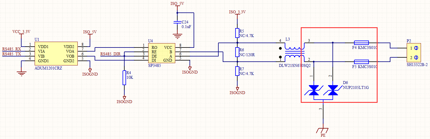
As shown in the figure below, PTC and TVS are used for RS485 overvoltage protection. The power supply voltage of the device is 24V. The RS485 chip selects MAX488, the normal working voltage is 5V, the maximum can withstand 12V, and the normal working current is less than 1mA. Choose the appropriate PTC and TVS .
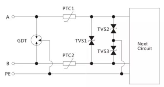
(1) PTC selection
Since the working current of RS485 is very small, choose the smallest PTC current. The key parameter is the trip time Trip. The smaller the trip, the better, and the smaller the trip time, the lower the power requirement for TVS, the smaller the package, and the higher the cost. low. After selection, the current and voltage of SMD1812B020TF meet the requirements, and the trip time Trip is the shortest, which is 0.02S.
(2) TVS selection:
- TVS voltage selection
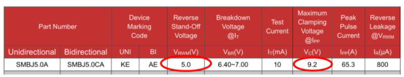
Since the working voltage VCC of RS485 is 5V and the limit voltage is 12V, the working voltage Vrwm of TVS is ≥5V, and the clamping voltage is ≤12V; SMBJ5.0A can be pre-selected. Vrwm=5V, Vc=9.2V.
- TVS power selection
a. Estimate the amount of heat that the actual TVS needs to withstand
Assuming that the TVS works at the maximum clamping voltage, the current flowing is the trip current of the fuse:
Qact=P*t=U*I*t=Vc*I trip*Tptc=9.2V*8*0.02S=1.472Jb. Estimate the actual power of the actual TVS
Since the power of the TVS test given by the manufacturer is measured under the pulse width of 1us, it is necessary to convert the above-mentioned estimated heat into the corresponding TVS power when 1uS.
Ptvs>Qact/1us=1.472J/1us=1472W
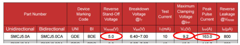
Converted into peak current: Ipp=P/Vc=1472W/9.2V=160ATherefore, TVS finally chose SMCJ5.0A with Vc=9.2V and Ipp=163.
Some friends think that the above calculation process is not derated. In fact, the above calculation process is basically based on extreme conditions, ignoring the exponential increase in resistance of PTC as the temperature rises, and the resistance on the PTC will share a large part of the voltage. In the later stage, the PTC was on the verge of breaking, and the withstand voltage drop of the TVS was almost zero. Therefore, not only is there no need to derate, even the power of TVS can be multiplied by the actual calculated coefficient of 0.5 to 0.8.
1.4. Summary
TVS has two limitations for overvoltage protection: small signal and low speed.
(1) Small signal problem
The small signal is easier to understand. Our circuit uses a PTC with a normal current of 0.2A, but the 160A TVS is used, which is close to 800 times. It is unimaginable that if a 2A PTC power port is used, the power of the TVS needs to exceed 15KW. The price is close to 10 yuan, this cost is almost no one can accept.
Since the PTC is self-recovering, it can work normally after the fault is removed, avoiding the trouble of frequent replacement, but the tripping time of the PTC is longer, which is equivalent to a 0.2A glass-sealed fuse. When the circuit reaches 8A, it is almost within 10ms. It can be tripped, and the shortest PTC is 200ms, which results in the TVS power must be selected to be larger, in order to insist on the PTC trip (PTC must fail before TVS to protect it).
(2) The problem of low speed
The junction capacitance of a general TVS is tens of pF to hundreds of pF. At the same power level, the lower the TVS voltage, the larger the junction capacitance. The power TVS used in the small signal port, unless it is a low-capacitance TVS, the conventional power TVS junction The capacitance will be in the tens of pF, so the rate of the small signal cannot be too high, preferably not more than 1Mbps.
(3) Accuracy issues
The calculation process mentioned above is basically estimated. This is because TVS and PTC are voltage and current sensitive devices, and the failure modes are thermal failures. Careful friends will find that the voltage, current, and current provided by the manufacturer’s TVS manual The temperature and other relations are given a rough graph, but no precise calculation formula is given.
Although accurate formulas are used in the calculations in this article, they are under extreme conditions. The actual selected TVS can be multiplied by a coefficient 0.5 to 0.8 than the calculated value. It is not a big problem. The actual test shall prevail. For example, in the above example, the 160A TVS is selected for calculation, and the actual test uses 100A to meet the requirements.
2. Reliable and efficient circuit
A simple overvoltage protection circuit can generally be realized by adding a TVS. When there is a momentary high-energy impact from the outside, it can suppress this energy. Although the power is high, thousands of W can be used, but the suppression time is very short and short.In case the device is damaged or the working voltage is higher than the normal working voltage for a long time, it will be powerless.
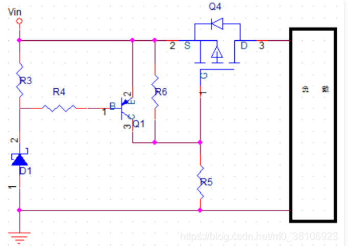
So the best way is to design a smart circuit, as shown below:
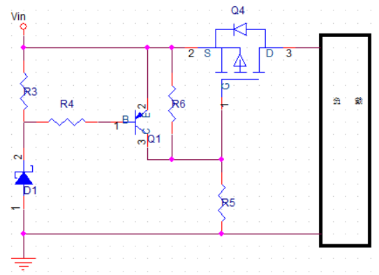
When Vin is at a normal input voltage, there is no reverse breakdown of the Zener tube, and the currents of R3 and R4 are basically zero. The Vbe of the PNP transistor is=0, that is, the PNP transistor is not conducting. The Vgs of the PMOS transistor Q4 is determined by the partial pressure of the resistors R5 and R6, and the PMOS transistor is turned on, that is, the power supply works normally.
When the Vin input is greater than the normal input voltage, at this time Vin>Vbr, the Zener tube is broken down, and the upper voltage is Vbr. The PNP transistor Q1 is turned on, VCE≈0, that is, Vgs≈0 of the PMOS tube, the PMOS tube is not turned on, and the circuit is open, that is, the overvoltage protection is realized.
If the accuracy is high, of course, a voltage detection IC can also be used to realize voltage monitoring.
Reference materials:
TVS selection, so that the elderly and newcomers can be handy!
Brother Laoyu teaches you to analyze the design of the overvoltage protection circuit. Have you got the essence?
[Dry goods sharing] TVS is used for conventional overvoltage protection
MOS tube anti-reverse connection and anti-overvoltage circuit
Intelligent Recommendation
Design of RS485 protection circuit
Design of RS485 protection circuit 1. Question: The RS485 interface of a recently designed board was burned down due to high voltage, which is terrible. You can see the picture. Figure 1 The scene of ...

Overvoltage protection (2)
Overvoltage protection circuit composed of CW136 The figure shows the overvoltage formed by CW136.protect the circuitWhen the supply voltage of the electronic device exceeds the rated voltage for some...

Overvoltage detection circuit
The schematic diagram of the over-voltage detection circuit is shown in the figure. When an overvoltage signal is generated, the varistor is broken down, showing a low resistance value even close to a...
PMOS tube overvoltage circuit
A simple overvoltage protection circuit can generally be realized by adding a TVS. When there is a momentary high-energy impact externally, it can suppress this energy. Although the power is high, tho...
Anti-reverse protection circuit design
Generally, it can be solved by using a diode in the positive pole of the power supply. However, due to the voltage drop of the diode, it will cause unnecessary loss to the circuit. Especially in the c...
More Recommendation
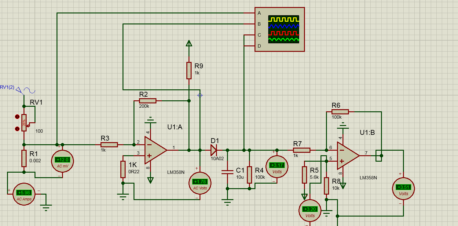
Overcurrent protection circuit design simulation
Overcurrent protection circuit design simulation figure 1 Figure 2 220 alternating current is sampled by the simulated load RV1 and R1, the signal is amplified by the operational amplifier 200 to ampl...

Simulation of overvoltage circuit formed by triode
Simulation of overvoltage circuit formed by triode This circuit has an overvoltage protection circuit composed of two transistors, four resistors and a Zener diode, as shown in Figure 1: The following...

Hardware design: circuit protection-TVS tube
Reference materials:TVSParameters and selection methods TVSParameter understanding Components Product Description of Shenzhen Shuokai Electronics Co., Ltd. TVS(Transient Voltage suppres...
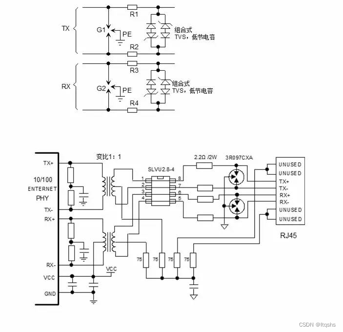
EMC-network port lightning protection circuit design
There are two ways to protect lightning at the network port: one is to give lightning current a drainage path, release the high voltage before the transformer, minimize the impact on the transformer a...
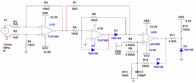
Circuit design, analysis, simulation 2: current detection and protection circuit simulation
Schematic diagram Note: V1 replaces the current sampling signal. Differential circuit simulation and analysis The differential circuit consists of U1D and peripheral components. The magnification is 1...