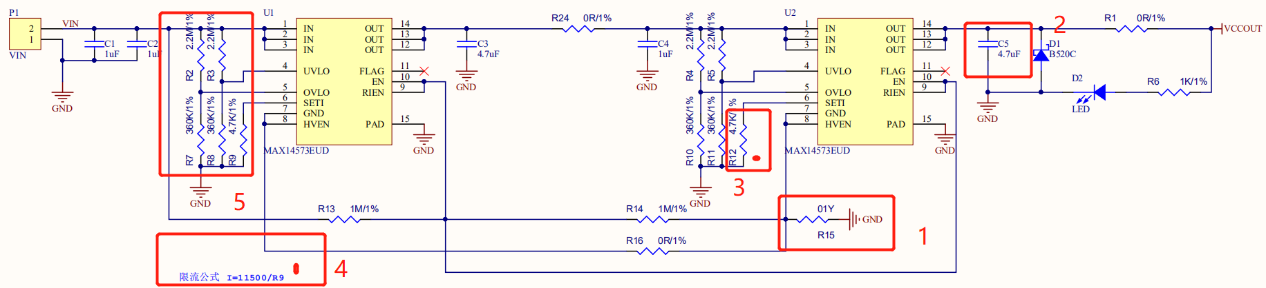
Overvoltage protection circuit composed of CW136
The figure shows the overvoltage formed by CW136.protect the circuitWhen the supply voltage of the electronic device exceeds the rated voltage for some reason,
Bring the CW136 to 5V between positive and negative, showing a low impedance state and triggering immediatelyThyristorTurn on, the short-circuit current can blow the fuse at a moment.
Thereby cutting off the power supply and achieving overvoltage protection of the electronic device.

It consists of a P-N-P-N four-layer semiconductor with three PN junctions in between.Thyristor conduction conditions are: plus forward voltage and gate with trigger current
The ideal solution is to use MOSFETs as switching and protection switches. The MOSFET has a milliohm-level conduction resistance, and the voltage drop caused by it is almost negligible. When the battery voltage is too low, the MOSFET can also be used to cut off the power supply path to protect the battery. But you need to design a special circuit to detect the voltage and drive the MOSFET gate. This can be done with standard voltage comparators, voltage references and discrete components, but this increases the component count and complexity of the circuit and increases static power consumption.

In addition, the MAX4842's overvoltage protection threshold is 4.4V-5.0V, which is also higher than the 4.2V upper limit voltage of a single-cell lithium battery.
The MAX4842 drives the gates of Q1 and Q2 to a high level to turn on the battery, and the battery supplies power to the load.
The MAX4842 is disabled, Q1, Q2 are turned off, and the load is powered by an external power supply.
Since it is on the external power supply path, it does not matter if it loses efficiency.

Hello everyone, has anyone done a circuit overvoltage protection scheme?
As shown in the figure, I intend to use Pmos to make the circuit protection switch. When the overvoltage (should be less than 15V) is detected, the power supply is cut off to protect the rear stage circuit (rated voltage 5V, 20mA), but I have not touched the mos. I don't know this scheme. Is it feasible. several questions:
1. How to choose MOS model parameters? (Circuit requirements up to 30V, mos on-resistance is small)
2, MOS circuit design methods, such as resistance values?
3. Is there a better overvoltage protection circuit scheme?
5V 20mA with a triode can be used, overvoltage protection:
1. Overvoltage disconnection (triode, MOS tube, relay),
2. Overvoltage absorption (voltage regulator, triode, MOS tube, varistor),
3. Overvoltage conversion (the voltage is automatically converted to the appropriate voltage to the subsequent stage).
Use TL431 plus positive and negative to replace your overvoltage detection circuit. ,
In addition, such a small current, with the S8050 TO-92 package can meet the requirements.
http://bbs.dianyuan.com/topic/677773

The input supply voltage is +-24V, which requires protection when the voltage exceeds 29V. I have now designed a +24V protection circuit.
But the negative power supply (-24V) stunned. Requires protection beyond -29V.How to do overvoltage protection of negative power supply? Thank you, hehe
In fact, the negative power supply is the same, the picture below is modified on your original picture.

This is what I thought last night, and it is similar to your thinking. However, the LM393 is open drain and you may not notice it.

In terms of overcurrent and overvoltage protection, Raychem's PolyZenTM component devices are integrated circuits consisting of precision Zener diodes and polymer positive temperature coefficient (PPTC) components. It is a protection device for preventing induced spike voltage, instantaneous high voltage, and misuse of the power adapter to cause overvoltage and overcurrent damage to the circuit. The internal structure is shown below.

During normal operation, the VIN input voltage is higher than the breakdown voltage VZ of the Zener diode, and the IFLT current is passed through the Zener diode to ground, and VOUT outputs a stable voltage. When there is an abnormal overvoltage input VIN, the IFLT of the Zener diode will generate an overcurrent. When there is an overcurrent on the device, its resistance changes from a low-resistance state to a high-impedance state, causing a large voltage drop across it. Increase, the VOUT output is basically unchanged, and the current IFLT flowing through the Zener diode is reduced, as shown in the following figure. The increase in voltage drop across the device protects both the Zener diode and the downstream circuitry. In addition, if there is a partial short circuit or short circuit fault in the protected downstream circuit, IOUT will increase, and the PPTC component will change from a low resistance state to a high resistance state, which can make the circuit get overcurrent protection.

PolyZen devices are polymer-protected precision Zener diode micro-integrated modules. These devices feature resettable protection against high-power fault events, while only 0.7W of power dissipation, eliminating the need for special heat sinks. PolyZen devices have a relatively smooth voltage and current response, which helps clamp the output voltage even when the input voltage and supply current vary. An advanced feature of the PolyZen micro-integrated module is the additional protection of its Zener diode and subsequent electronics from the resistive nonlinear polymer PTC (Positive Temperature Coefficient) layer. The PTC layer is fully integrated into the device, thermally coupled to the diode, and electrically connected in series between VIN and the diode clamped VOUT. The advanced PTC layer responds to diode heating or overcurrent events by switching from a low-impedance state to a high-impedance state (also known as "action"). The action of the PTC will limit the current and create a voltage drop, which helps protect the Zener diode and subsequent electronic components. This integrated PTC effectively enhances the power handling capability of the diode.
LTC4360-1 / LTC4360-2 - Overvoltage Protection Controller
Characteristics
- 2.5V to 5.5V operating voltage
- Overvoltage protection up to 80V
- No input capacitor or TVS (transient voltage suppressor) is required for most applications
- 5.8V overvoltage threshold with 2% accuracy
- <1μs overvoltage shutdown time, step-by-step shutdown
- Control N-channel MOSFET
- Adjustable power-up dV/dt limits inrush current
- Reverse Voltage Protection (LTC4360-2)
- Power good output
- Low current shutdown mode (LTC4360-1)
- Available in a tiny 8-pin SC70 package


description
LTCThe 4360 overvoltage protection controller protects the 2.5V to 5.5V system from power supply overvoltage damage. It is designed for portable devices with a variety of power options, including wall adapters, car battery adapters, and USB ports.
The LTC4360 is used to control an external N-channel MOSFET in series with the input supply. During an overvoltage transient, the LTC4360 can turn off the MOSFET within 1μs, thereby isolating downstream components from the input supply. Inductive cable transients are attenuated by MOSFETs and load capacitors. In most applications, the LTC4360 provides protection against transient voltages up to 80V without the need for transient voltage suppressors or other external components.
The LTC4360 features a delayed start and adjustable dV/dt ramp for limiting inrush current. OnePWRGDPins are provided for VINPower good monitoring. After an overvoltage condition, the LTC4360 will automatically restart after a start delay. LTC4360-1 has a controlledONThe soft stop function of the pin, while the LTC4360-2 controls an optional external P-channel MOSFET to provide negative voltage protection.
application
- USB protection
- Handheld computer
- Cellular phone / smartphone
- MP3 / MP4 player
- Digital camera
LTC4361-1 / LTC4361-2 - Overvoltage / Overcurrent Protection Controller
Characteristics
- 2.5V to 5.5V operating voltage
- Overvoltage protection up to 80V
- No input capacitor or TVS (transient voltage suppressor) is required for most applications
- 5.8V overvoltage threshold with 2% accuracy
- 50mV overcurrent circuit breaker with 10% accuracy
- <1μs overvoltage shutdown time, step-by-step shutdown
- Control N-channel MOSFET
- Adjustable power-up dV/dt limits inrush current
- Reverse voltage protection
- Power good output
- Low current shutdown mode
- Locked off after overcurrent (LTC4361-1) or automatic retry (LTC4361-2)
- With 8-pin ThinSOTTMPackage and 8-pin (2mm x 2mm) DFN package


description
LTCThe 4361 overvoltage/overcurrent protection controller protects the 2.5V to 5.5V system from input power supply overvoltage. It is designed for portable devices with a variety of power options, including wall adapters, car battery adapters, and USB ports.
The LTC4361 is used to control an external N-channel MOSFET in series with the input supply. During an overvoltage transient, the LTC4361 can turn off the MOSFET within 1μs, thereby isolating downstream components from the input supply. Inductive cable transients are attenuated by MOSFETs and load capacitors. In most applications, the LTC4361 provides protection against transient voltages up to 80V without the need for transient voltage suppressors or other external components.
The LTC4361 features a delayed start and adjustable dV/dt ramp for limiting inrush current. OnePWRGDPins are provided for VINPower good monitoring. LTC4361 has a controlledONThe soft stop function of the pin drives an optional external P-channel MOSFET to provide negative voltage protection. After an overvoltage condition, the LTC4361 will automatically restart after a start delay. After an overcurrent condition, the LTC4361-1 remains off and the LTC4361-2 will automatically restart after a 130ms start-up delay.


description
LTCThe 4365 protects applications where the power supply input voltage is likely to be too high, too low, or even negative. The device implements this protection by controlling the gate voltage of a pair of external N-channel MOSFETs to ensure that the output is within a safe operating range.
The LTC4365 can withstand voltages from -40V to 60V and has a 2.5V to 34V operating range with a current consumption of only 125μA during normal operation.
Two comparator inputs are configured with an external resistive divider to provide overvoltage (OV) and undervoltage (UV) setpoints. A shutdown pin is responsible for providing external control for enabling and disabling the MOSFET and placing the device in a low current shutdown state. A fault output provides the state of the GATE pin that is pulled low. A fault is indicated when the device is at a standstill or the input voltage is outside the UV and OV setpoints.

When Vi exceeds a certain voltage, the TL431 triggers to turn on the thyristor, generating a large instantaneous current, and blowing the fuse to protect the rear pole circuit. V protection point = (1 + R1/R2) Vref


When TL431The voltage at the reference input is lower than2.5VFlow throughTL431The current does not exceed400 μA, so R3The pressure drop on the top is small. When the power supply voltage is increasedTL431The voltage at the reference input exceeds2.5VTime,TL431 Turn on,R3The voltage drop across it increases until the thyristor turns on.
The operating voltage of this circuit is more accurate. However, bidirectional thyristors must be used, and ordinary unidirectional thyristors cannot work.

Further eliminate the effect of temperature on the thyristor.


When Vi exceeds a certain voltage, the TL431 triggers to turn on the thyristor, generating a large instantaneous current, and blowing the fuse to protect the rear pole circuit. V protection point = (1 + R1/R2) Vref

The TL431 contains a 2.5V reference internally, so when the output feedback is introduced at the REF terminal, the device can control the output voltage by shunting a wide range from cathode to anode. As shown in the circuit of Figure 2, when the resistance values of R1 and R2 are determined, the two introduce feedback to the partial pressure of Vo. If V o increases, the feedback amount increases, and the shunt of TL431 increases, which in turn leads to Vo. decline. Obviously, this deep negative feedback circuit must be stable at VI equal to the reference voltage, at which time Vo = (1 + R1/R2) Vref. Selecting different values of R1 and R2 results in any voltage output from 2.5V to 36V, in particular, when R1 = R2, Vo = 5V. It should be noted that the necessary condition for the TL431 to operate when selecting the resistor is that the current through the cathode is greater than 1 mA.