PMOS tube overvoltage circuit
tags: circuit design schematic diagram power supply hardware engineering embedded hardware overvoltage protection
A simple overvoltage protection circuit can generally be realized by adding a TVS. When there is a momentary high-energy impact externally, it can suppress this energy. Although the power is high, thousands of W can be used, but the suppression time is very short. In case the device is damaged or the working voltage is higher than the normal working voltage for a long time, it will be powerless.
So the best way is to design a smart circuit, as follows:
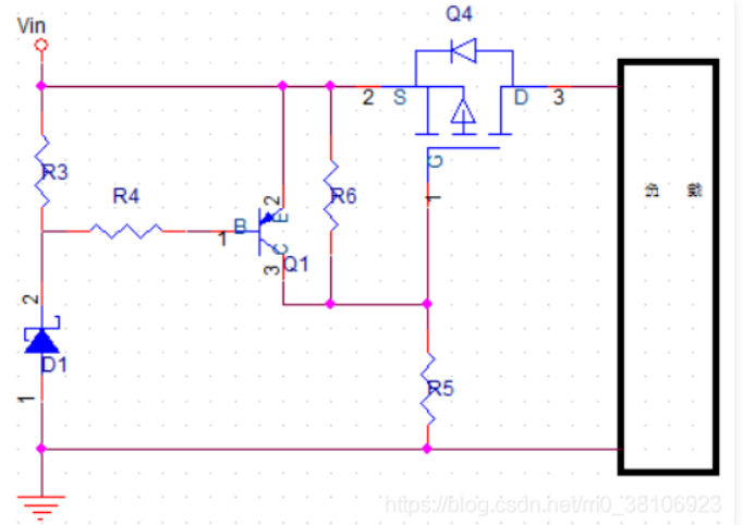
When Vin has a normal input voltage, the Zener tube has no reverse breakdown, and the current of R3 and R4 is basically 0. Vbe=0 of the PNP transistor, that is, the PNP transistor is not conducting. The Vgs of the PMOS transistor Q4 is determined by the voltage divider of the resistors R5 and R6, and the PMOS transistor is turned on, that is, the power supply works normally.
When the Vin input is greater than the normal input voltage, Vin>Vbr at this time, the Zener tube is broken down, and the voltage on it is Vbr. The PNP transistor Q1 is turned on, VCE≈0, that is, Vgs≈0 of the PMOS transistor, the PMOS transistor is not turned on, and the circuit is disconnected, which realizes overvoltage protection.
If the precision requirement is high, of course, a voltage detection IC can also be used to realize voltage monitoring.
Disclaimer: This article is reproduced from the Internet, and the copyright belongs to the original author. If the videos, pictures, and text used in this article involve the copyright of the work, please inform us as soon as possible. The content of this article is the original author's opinion, which does not mean that this official account agrees with his opinion and is responsible for its authenticity.Reference text
Intelligent Recommendation
PMOS switch selection and circuit diagram
The choice of MOSFET is first. There are two main types of MOSFET: N-channel and P-channel. In power systems, MOSFETs can be considered as electrical switches. When a positive voltage is applied betwe...
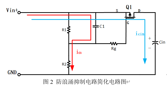
PMOS anti-surge suppression circuit
PMOS anti-surge suppression circuit 1. Source of surge current 2. Analysis of anti-surge suppression circuit 2.1 Circuit principle 2.2 Influencing factors 2.2.1 Influence of RC parameters 2.2.2 Influe...
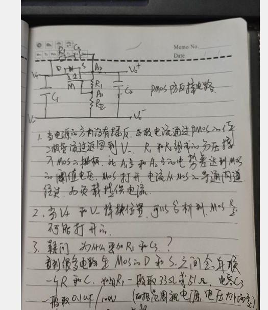
PMOS anti-reverse connection circuit
I posted a PMOS anti-reverse connection circuit, but I haven’t figured out the function of R1 and C3 connected in parallel between D and S of the mos tube. I checked it on the Internet, and some...

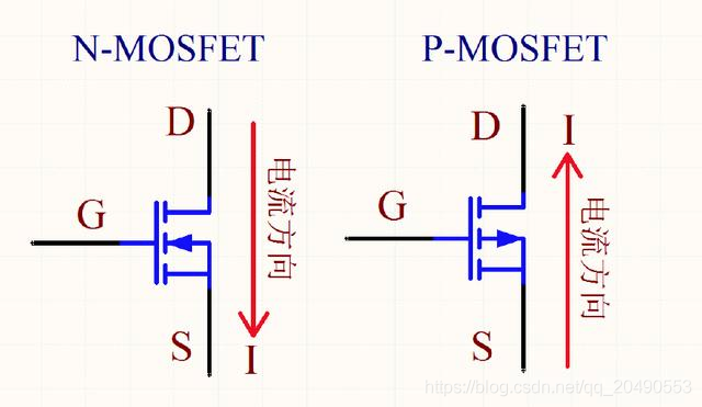
Ingenious memory method for distinguishing PMOS tube and NMOS tube
There are three pins of the MOS transistor: source S (source), gate G (Gate) and drain (Drain), but in practical engineering applications, it is often impossible to distingu...
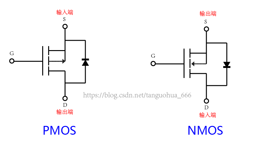
Ingenious memory method to distinguish PMOS tube and NMOS tube
There are three pins of MOS tube: source S (source), gate G (Gate) and drain (Drain), but in practical engineering applications, it is often impossible to distinguish between PMOS tube and NMOS tube, ...
More Recommendation
Why use NMOS tube for bootstrap switch instead of PMOS tube
Does the bootstrap switch limit the input signal range? The difference between NOMS tube and PMOS tube First of all, in terms of performance alone, the performance of pmos is not as good as nmos. Beca...

Why is MOS tube inverter to construct a PMOS tube and NMOS?
Why is MOS tube inverter to construct a PMOS tube and NMOS? In CMOS Analog Circuit Design, Phillip E. Allen, inverter covers a series of circuits as shown below. In fact, any enlargement is negative a...
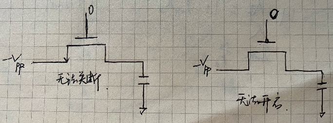
NMOS tube and PMOS tube are used as switch control circuits
Article Directory 1 MOS tube conduction and cut-off principle 2 MOS tubes are used for upper and lower tubes 3 NMOS tube application 4 PMOS tube application 1 MOS tube conduction and cut-off principle...
Overcurrent overvoltage protection for protection circuit series
Overcurrent overvoltage protection for protection circuit series The article was transferred from:http://www.eetop.cn/blog/html/65/1196765-6648753.html The last study was summarizedProtection de...

The original understanding of 5V overvoltage protection circuit
Baidu for a long time found that this protection circuit exists, but the related principle description is very blank, or the description is a bit confusing... So I write this article to record the exp...