HDL/FPGA study notes 22: the use of Vivado dual-port RAM IP core
tags: HDL/FPGA study notes fpga verilog
1. Introduction to dual-port RAM
Double mouthRAM(dual port RAM)Widely used in heterogeneous systems, throughDual port RAM, Chips with different hardware architectures can realize data interaction, so as to realize communication. For example, in general,ARM and DSPCommunication between you can useDual port RAMachieve,ARMbyEBIBus connected toDual port RAMofAmouth,DSPbyEMIFBus (can also beuPPBus, depending on speed requirements) connected toDual port RAMofB , the two can operate on the same storage area to realize the data exchange between the two.
But becauseDual port RAMofAMouth andBBoth ports can operate on the same memory address, which leads to a problem-if both parties in communication read and write to the same address at the same time on two ports, conflicts will occur. There are two ways to solve this problem.
- One is that the two parties in the communication ensure that they will not read and write the same address at the same time.
ARM and DSPThe writable address range is partitioned, regardless of whether any party finishes writing the data throughIOSend interrupt to notify the other party, and the other party reads data (Ping Pong RAMOperation), this is more reliable; - Another way is to
FPGASet to writebusySignal to achieve synchronization of writing at both ends.
inFPGABuildDual port RAMThere are two methods, one is to usedistributed RAMBuild, the other is to useBlock RAMConstruct. in short,Block RAMIs to useFPGAThe whole pieceDual port RAMResources, whiledistributed RAMThen useFPGAThe logical resources in the patchwork are formed. The general principle is that for larger storage applications, it is recommended to useBlock RAM; Sporadic smallRAM, Generally usedistributed RAM。
2. RAM IP core generation and configuration
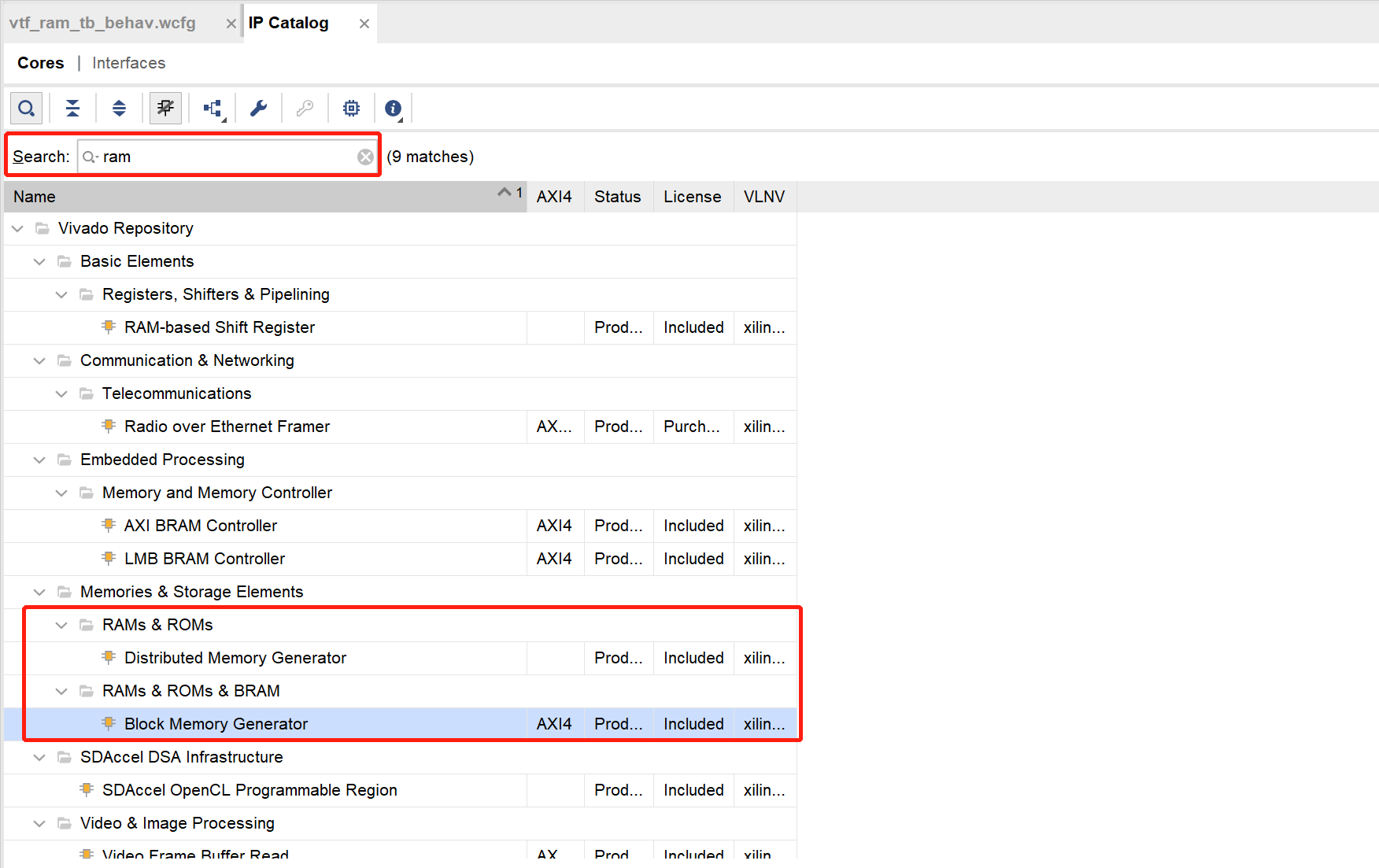
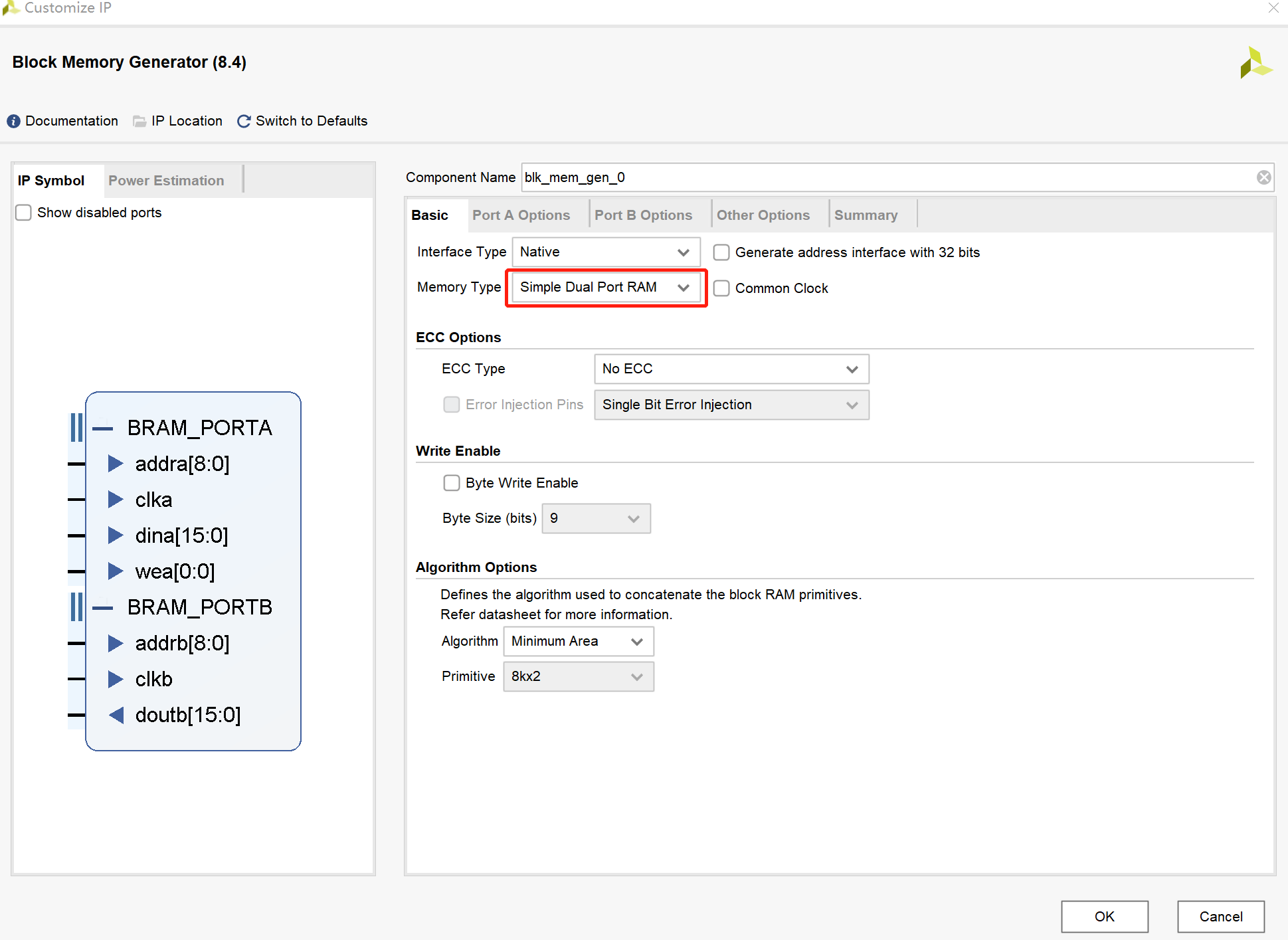
There are three types of block RAM: single-port RAM, simplified dual-port RAM and true dual-port RAM.
- Single-port RAM has only one port (port A), which can read and write to port A.
- Simplified dual-port RAM has two ports (A and B ports), but the A port can only perform write operations and cannot perform read operations, while the B port can only perform read operations but cannot perform write operations.
- True dual-port RAM has two ports (A and B ports), and both A and B ports can perform read and write operations.
What we chose above is to simplify dual-port RAM.
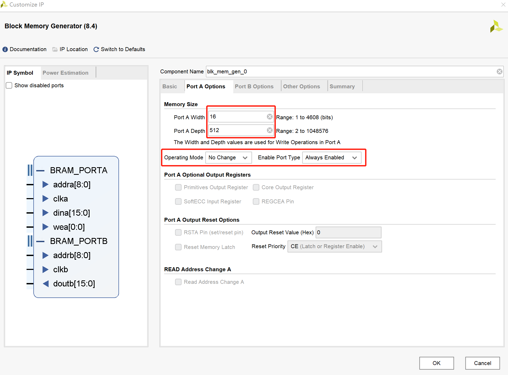
For the Operating Mode option of input port A, please refer to the following article for details:
“WRITE_FIRST”Mode, during write operation, the output port will output the currently written data.“READ_FIRST”Mode, during write operation, the output port will output the original data of the current write address.“NO_CHANGE”Mode, during write operation, the output port will keep the original value unchanged. The output port will only change during the read operation.
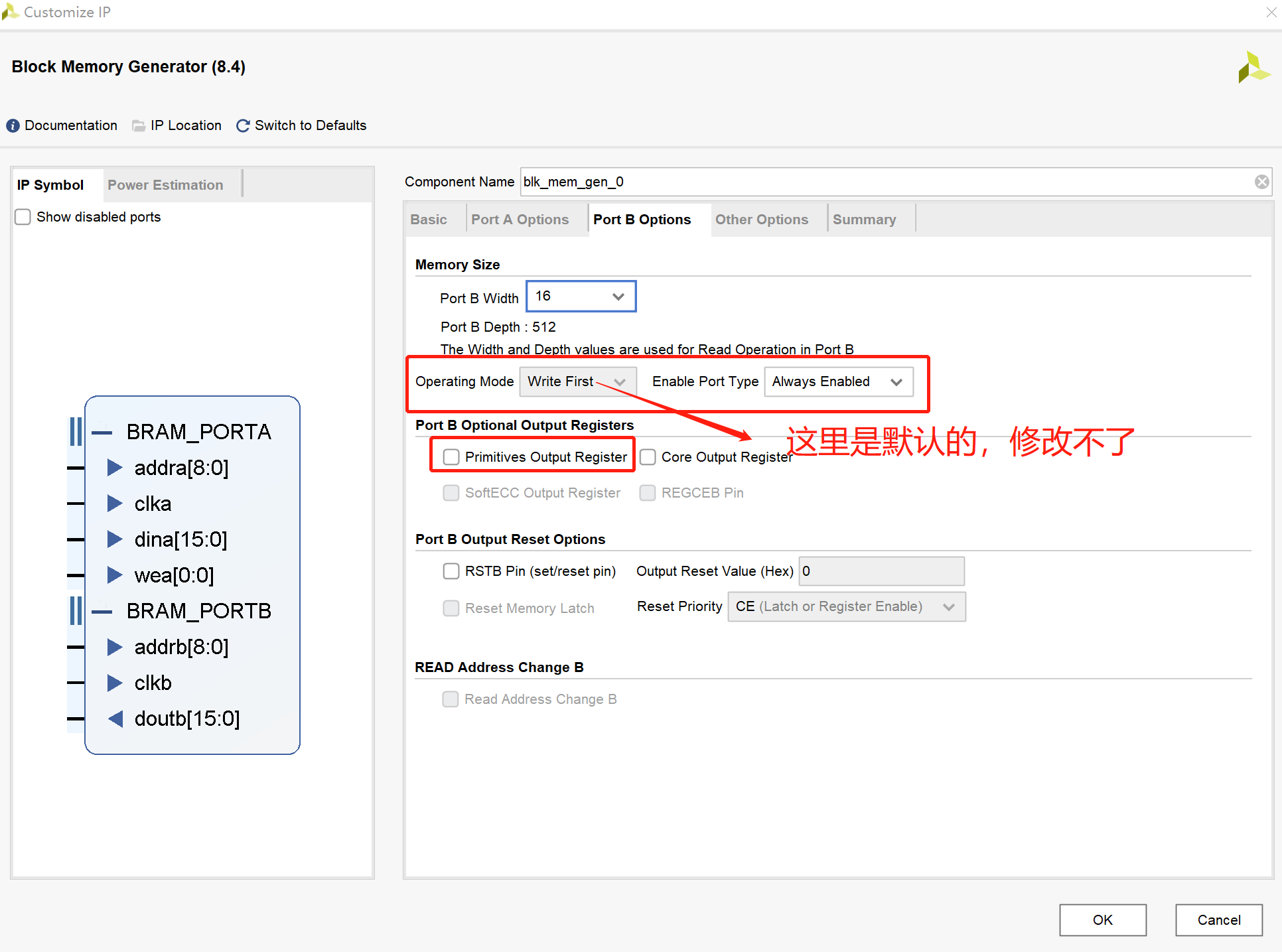
About the Primitives Output Registers option of output port B:
If this option is not checked, then under normal circumstances, when the address is sent at the first clock, the data will be fetched and sent out to RAM at the second clock.But when this option is checked, the data will be delayed by two clocks and sent out on the third clock. This is the timing in the case of fetching data. When storing data, only the address and data need to be in the same clock.
Three, examples
The function implemented in the following example is: for a dual-port RAM that has been configured with a data bit width of 16 and a depth of 512, the write operation of address increment is performed first, and then the read operation of address increment is performed immediately. Among them, the read operation is delayed by one clock cycle than the write operation, which can also prevent the read and write operations from acting on the same address at the same time; both ports AB are set to always be enabled,But it should be noted that input port A has an additional write enable wea。
1. RTL code
`timescale 1ns / 1ps
//
module ram_test(
			input clk,		          	//50MHz clock
			input rst_n	             	//Reset signal, active low
		);

//-----------------------------------------------------------
reg		[8:0]  		w_addr;	   		//RAM PORTA write address
reg		[15:0] 		w_data;	   		//RAM PORTA write data
reg 	      		wea;	    	//RAM PORTA enable
reg		[8:0]  		r_addr;	  	 	//RAM PORTB read address
wire	[15:0] 		r_data;			//RAM PORTB read data

//Generate RAM PORTB read address
always @(posedge clk or negedge rst_n)
begin
  if(!rst_n)
	r_addr <= 9'd0;
	/*
         Here is to delay the read address by one cycle than the write address
         You might think, when w_addr=1 is not equal to 9'd0, doesn't r_addr also increase by 1 and become 1?
         How can a delay of one clock cycle be realized?
         That's because r_addr is a register type variable, and the value at this time can only be collected in the next clock cycle.
  */
  else if (|w_addr)			//w_addr bit or, not equal to 0
    r_addr <= r_addr+1'b1;
  else
	r_addr <= 9'd0;
end

//Generate RAM PORTA write enable signal
always@(posedge clk or negedge rst_n)
begin
  if(!rst_n)
  	  wea <= 1'b0;
  else
  begin
     if(&w_addr) 	//The bits of w_addr are all 1, a total of 512 data are written, and the writing is complete
        wea <= 1'b0;
     else
        wea	<= 1'b1;  //ram write enable
  end
end

//Generate the address and data written by RAM PORTA
always@(posedge clk or negedge rst_n)
begin
  if(!rst_n)
    begin
      w_addr <= 9'd0;
      w_data <= 16'd0;
    end
  else
  begin
    if(wea)//ram write enable is valid
      begin
        //When the write address is all 1, it means that 512 data has been written, and the write enable is not necessary.
        if (&w_addr)
          begin
          w_addr <= w_addr ;	//Keep the value of address and data, write to RAM only once
          w_data <= w_data ;
          end
        else
          begin
          w_addr <= w_addr + 1'b1;
          w_data <= w_data + 1'b1;
          end
      end
  end
end

//-----------------------------------------------------------
//Instantiate RAM
ram_ip ram_ip_inst (
  .clka      (clk          ),     // input clka
  .wea       (wea          ),     // input [0 : 0] wea
  .addra     (w_addr       ),     // input [8 : 0] addra
  .dina      (w_data       ),     // input [15 : 0] dina
  .clkb      (clk          ),     // input clkb
  .addrb     (r_addr       ),     // input [8 : 0] addrb
  .doutb     (r_data       )      // output [15 : 0] doutb
);

endmodule
2. Simulation program
`timescale 1ns / 1ps

module vtf_ram_tb;
// Inputs
reg clk;
reg rst_n;


// Instantiate the Unit Under Test (UUT)
ram_test uut (
	.clk	(clk),
	.rst_n	(rst_n)
);

initial
begin
	// Initialize Inputs
	clk = 0;
	rst_n = 0;

	// Wait 100 ns for global reset to finish
	#100;
      rst_n = 1;

 end

always #10 clk = ~ clk;   //20ns a period, generate 50MHz clock source

endmodule
3. Simulation results

It can be seen that when reading data, the output data is also delayed by one clock cycle from the input address! ! !
Intelligent Recommendation
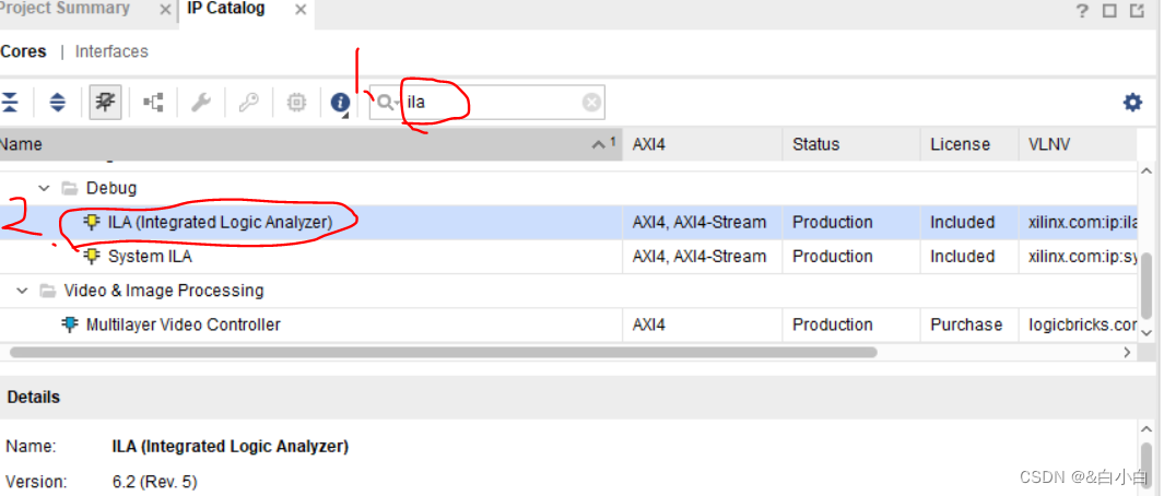
【Study Notes-FPGA】Calling logic analyzer IP core in vivado
Personal notes. When using vivado, we often use IP cores to implement it, such as mathematical operations (adders, subtracters, multipliers, etc.), and we can also use the IP core of the logic analyze...

Use of block ram in xilinx fpga-use of simple dual-port ram
Use of block ram in xilinx fpga-use of simple dual-port ram clka is the clock of the input port wea read and write control terminal, high for writing, low for reading addra write address dina Data to ...
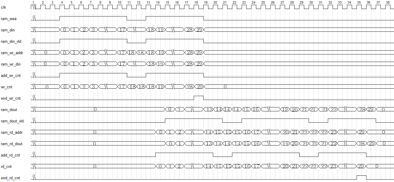
Detailed explanation of FPGA RAM, the use of pseudo dual-port RAM
In terms of flexibility, the pseudo-dual-port RAM is just between the single-port RAM and the real dual-port RAM, but it has to be said that it is the most widely used configuration type in RAM, and i...

Detailed explanation of FPGA RAM, the use of true dual-port RAM
True dual-port RAM IPpractise True dual-port RAM can be said to be the most flexible RAM IP core, because it gives users the largest design space, and two ports that can independently read and write a...
FPGA learning notes [use Vivado built-in IP core]
Clock IP core Vivado has built-in clock IP cores implemented using the clock resource in the FPGA, which can achieve divide, frequency, adjustment phase, control duty cycle. You can use clock IP check...
More Recommendation
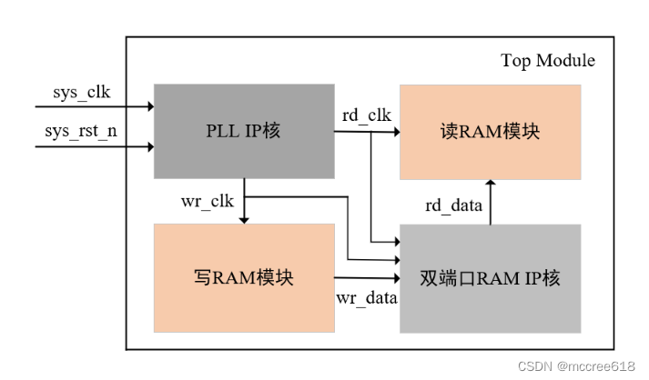
Dual -port RAM IP core module based on Quartus II
Design system frame diagram 1. Create a dual -port RAM IP core In order to achieve synchronous operations across the clock domain, the PLL core module is also required to obtain a clock of 50MHz and 2...
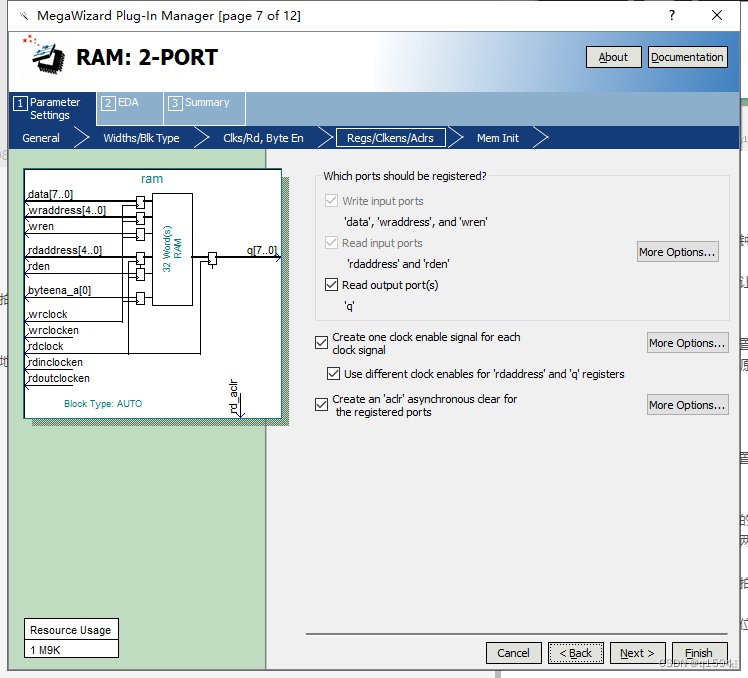
FPGA IP core RAM
1. Introduction to RAM RAM is the abbreviation of Random Access Memory (Random Access Memory), which is a volatile memory. When RAM is working, data can be written or read from any specified address a...

Vivado in ROM / RAM IP core using
Adding IP core Click onFlow NavigatormiddleIP CatalogOpen the window to add IP core. Block MemoryA block storage device, there is a needDistributed Memory Generator parameter settings Setting paramete...

Vivado IP core Ram Block Memery Generator
Vivado IP core Ram Block Memery Generator Table of contents Foreword 1. Configuration step Second, simulation 1. Top code 2. Simulation code Third, simulation analysis Summarize Foreword This introduc...

Dual-port RAM, worthy of study
FPGA design process, good use dual-port RAM, is a method for improving the efficiency. The official dual-port RAM is divided into simple dual-port RAM and true dual-port RAM. Simple dual-port RAM is o...