HDL/FPGA study notes twenty-four: the use of Vivado ROM IP core
tags: HDL/FPGA study notes fpga verilog
1. ROM IP core configuration
ROM is much simpler than the RAM mentioned earlier, because it only has a port for reading data and no port for writing data. However, it can still be configured as a single port or dual port, where the dual port refers to the port for reading data. Because it's relatively simple, I won't introduce too much here. The following is the configuration of the ROM IP core of my experiment:
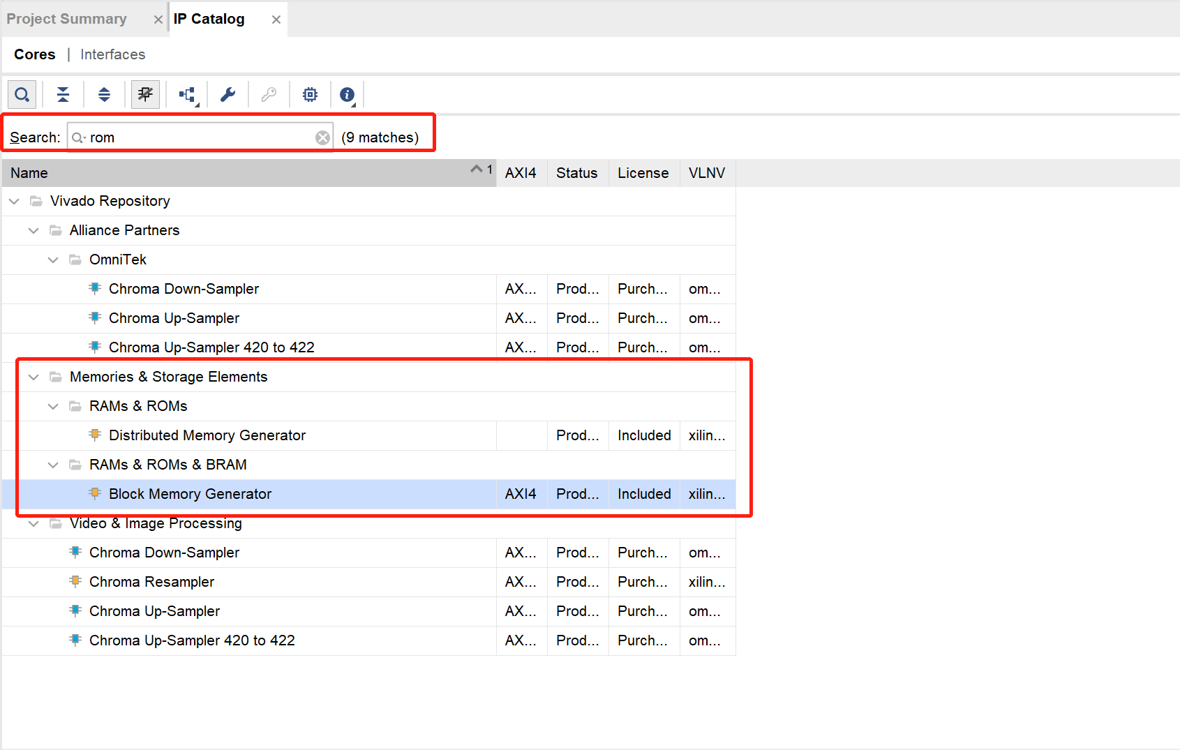
1. Find ROM IP core
As you can see, it is actually the same as the previous RAM.
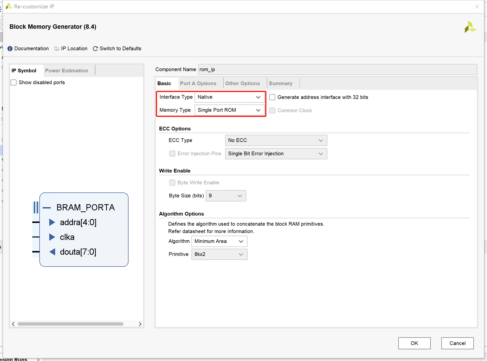
2. Choose single-port ROM
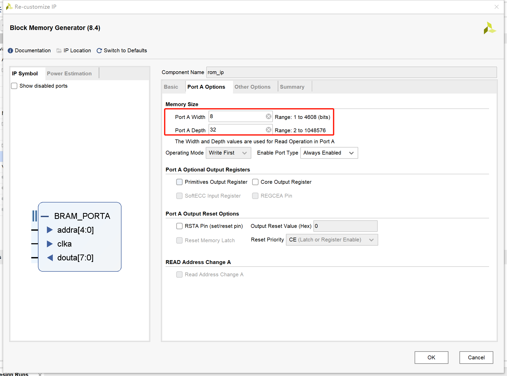
3. Set the data bit width and depth
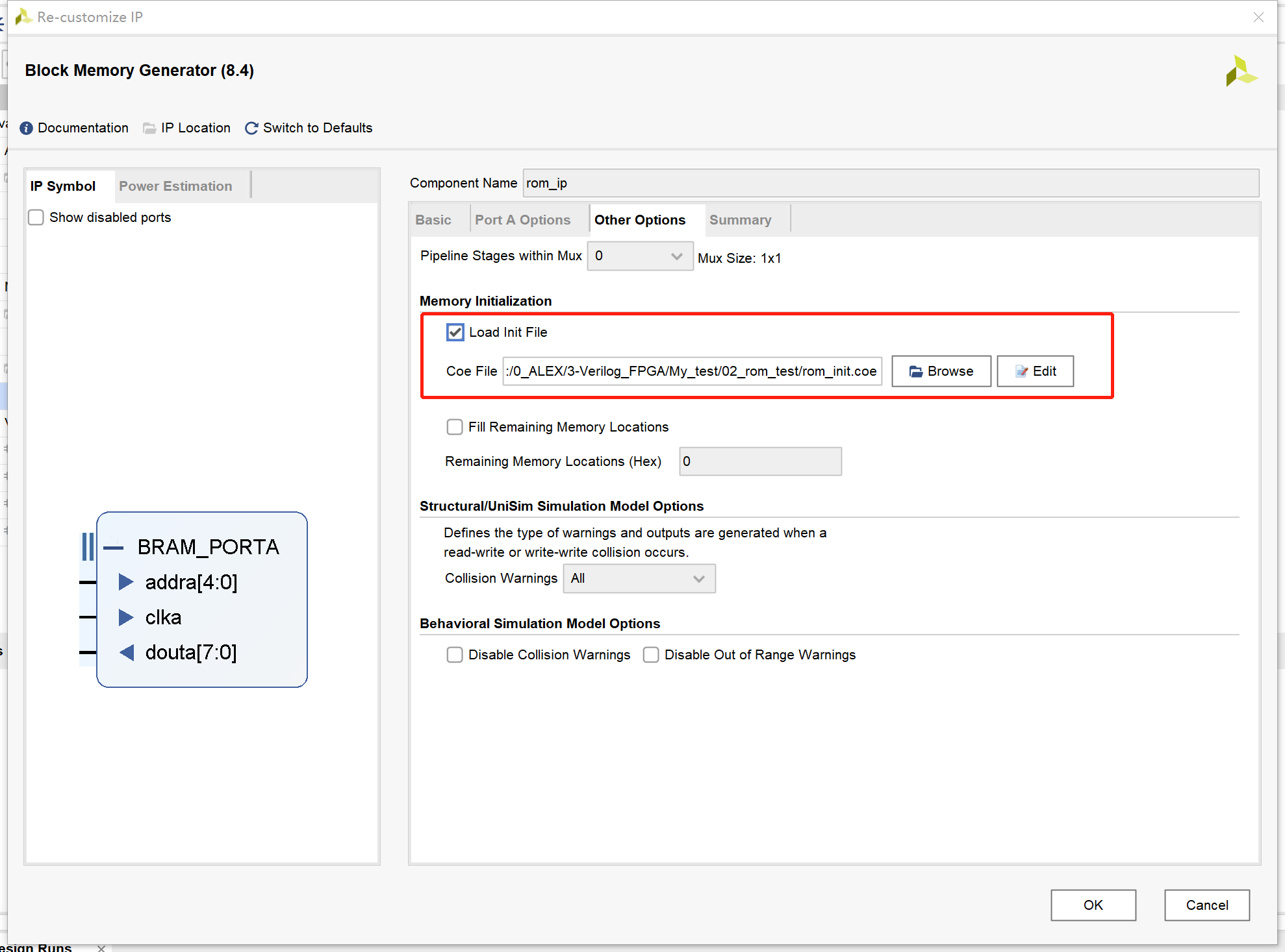
4. Initialize ROM
Used here iscoeFile, the content of the file is as follows:
MEMORY_INITIALIZATION_RADIX=16; //The data format indicating the ROM content is hexadecimal
MEMORY_INITIALIZATION_VECTOR=
11,
22,
33,
44,
55,
66,
77,
88,
99,
aa,
bb,
cc,
dd,
ee,
ff,
00,
a1,
a2,
a3,
a4,
a5,
a6,
a7,
a8,
b1,
b2,
b3,
b4,
b5,
b6,
b7,
 b8; //Each data is separated by a comma or a space or a newline character, and a semicolon is added after the last data
2. Examples
In this example, we simply read the data in the ROM one by one, and the read data address is incremented.
1. RTL code
`timescale 1ns / 1ps

module rom_test(
	input sys_clk,	//50MHz clock
	input rst_n		//Reset, active low
    );

wire [7:0] rom_data;	  //ROM read data
reg	 [4:0] rom_addr;      //ROM input address

//Generate ROM address to read data
always @ (posedge sys_clk or negedge rst_n)
begin
    if(!rst_n)
        rom_addr <= 10'd0;
    else
        rom_addr <= rom_addr+1'b1;
end
//Instantiate ROM
rom_ip rom_ip_inst
(
    .clka   (sys_clk    ),      //inoput clka
    .addra  (rom_addr   ),      //input [4:0] addra
    .douta  (rom_data   )       //output [7:0] douta
);
endmodule
2. Simulation program
`timescale 1ns / 1ps

module vtf_rom_tb;
// Inputs
reg sys_clk;
reg rst_n;


// Instantiate the Unit Under Test (UUT)
rom_test uut (
	.sys_clk	(sys_clk),
	.rst_n		(rst_n)
);

initial
begin
	// Initialize Inputs
	sys_clk = 0;
	rst_n = 0;

	// Wait 100 ns for global reset to finish
	#100;
      rst_n = 1;

 end

always #10 sys_clk = ~ sys_clk;   //20ns a period, generate 50MHz clock source

endmodule
3. Simulation results

It can be seen that the read data and the abovecoeThe content in the file is the same, indicating that the experiment was successful! ! !
Intelligent Recommendation
FPGA IP core ROM
1. ROM introduction ROM is the abbreviation of Read-Only Memory, a solid-state semiconductor memory that can only read out data stored in advance. The ROM or RAM generated by IP cores in FPGAs are gen...
[ROM IP] Vivado ROM IP core call experiment
ROM IP nuclear call experiment 1. ROM IP Nuclear Introduction The ROM is an abbreviation of read only memory, is a solid-state semiconductor memory that can only be read out in advance. Its feature is...

Vivado in ROM / RAM IP core using
Adding IP core Click onFlow NavigatormiddleIP CatalogOpen the window to add IP core. Block MemoryA block storage device, there is a needDistributed Memory Generator parameter settings Setting paramete...

Vivado IP core ROM DIST_MEM_GEN Usage
Distributed Memory Generator is an IP core that implements stored with LUT, RAM. This article discusses only the use of the ROM. Use of dist_mem_gen: It can be used as a large lookup table or in async...
Vivado study notes four
Vivado program curing When playing with FPGA development board for the first time, you will encounter this situation. The program written in advance is successfully compiled and downloaded to the boar...
More Recommendation

Vivado development environment, the COE file on the ROM IP core
DDS in the development process, we need to think well in advance of the COE added to the ROM file, follow these steps: 1. Open ROM IP core in Vivado in, where we choose Single ROM; 2. In the port A op...
Xilinx-ZYNQ7000 Series - Study Notes (4): Custom IP Core in vivado
Xilinx-ZYNQ7000 Series - Study Notes (4): Custom IP Core in vivado First, PWM First we write a pwm module for encapsulation into an IP core. Second, the establishment of vivado project 1. We created a...

YunSDR Y550 study notes 3.4 Vivado 18.3-IP core RAM
This content is learned from the leader ZYNQ's FPGA development guide V1.0 1. Introduction to RAM IP core The block RAMs inside Xilinx 7 series devices are all True Dual-Port RAM (TDP), and both ports...
vivado dds IP core notes
vivado dds IP core notes The DDS IP core can choose three configurations in the GUI interface provided by vivado: Phase Generator and SIN/COS LUT (DDS) SIN/COS LUT only, Phase Generator Here, record t...
Use AXI_Quad_SPI IP core in vivado
New vivado project Open the vivado software, I am using vivado2019.1 here, click create project to create a new project. Click next to continue to the next step. Enter the project name and project fil...