DesignWare_APB_GPIO module DUT&Testbench simulation
tags: FPGA Vivado APB_GPIO Embedded hardware FPGA development arm System architecture Functional testing
DW_APB_GPIO module DUT&Testbench simulation of ip test
Synopsys' gpio is a component of DesignWare Advanced Peripheral Bus (DW_apb), confirm to ARM's AMBA specification 2.0. .
1. Learn to read DW_apb_gpio_databook (data sheet can be downloaded from the homepage)
In fact, we are very familiar with GPIO and are used more frequently in ARM devices. We start using STM32 or Raspberry Pi. It is the most basic embedded interface. When used as input ports, we can read external data through them, and when used as output ports, we can control the connected peripheral devices through them output high or low levels. In layman's terms, GPIO is used to control pins. So the previous experience of using GPIO is also applicable here. We still operate GPIO through registers.
1.1 Overview:
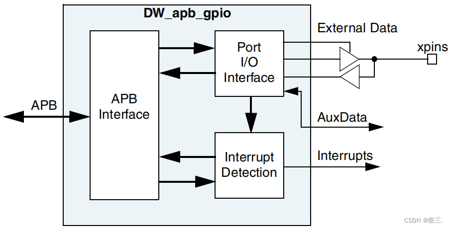
Synopsys' DW_apb_gpio is an integral part of DesignWare's advanced peripheral bus. Let's use this diagram to analyze the gpio IP.

You can see that these small IPs can be hung on the APB bus, APB advanced peripheral bus, as the name suggests, is mainly used to connect between low-bandwidth peripherals, such as UART and GPIO, which can be connected to it. Advanced peripheral buses do not support multiple main modules like high-performance buses. The only main module in the APB is the APB bridge.
Going back to the ip itself, configuring an IO requires registers. According to experience, we use configuration registers to select pin functions and use data registers to read/write port data.Generally, when we use GPIO to control peripherals, we configure a pin as an output or input, and then write 0 or 1 in the data register to output a high or low level. If set to input, it is generally used for address control. The same is true in adb_gpio. For example, for the gpio_swporta_dr register, if some bits are set to output, the value of the register will be output.
1.2 Function:
The features of DW_GPIO include: 1. Interface between APB and APB bridge
2. External data interface
3. Auxiliary hardware data interface
4. Interrupt the interface
It is best to generate the APPLY after workspace, and compare it with the component.v below src to see, for example, what signal will be generated. See how many generated signals are in the code. Then he will also have comments. For students who have just read these IPs, if they don’t understand the comments, they can combine them with the databook and may also combine them with the Block Diagram. The block diagrams of other IPs are also like GPIO. Generally, in the first chapter of the manual, there will be a DW_apb_component Block Diagram.
1.3 Features:

DW_GPIO features include:
1. There are 128 independent configuration signals
2. Four ports from A to D, can be configured separately
3. Each signal has a separate data register and a data direction register
4. Configurable hardware and software control for each signal bit
5. Configurable interrupt mode for port A
6. Configurable dejitter logic with external slow clock to eliminate jitter interrupts
7. GPIO component type register
8. GPIO component version register
9. Configurable reset value on the output signal
2. Simulation
Be prepared before simulation and download the genuine Synopsys software coreConsultant.
2.1 Workspace Directory Contents:
Learn about the code structure, open coreConsultant, and view the generated code structure after establishing Workspace.

Here I have made a structural map, you can take a look:

2.2 Function Description:

GPIO IP can be divided into software control mode and hardware control mode. In software control mode, the direction of external I/O is controlled by the write of the Portx data direction register (gpio_swportx_ddr). The written data is transmitted to the output signal gpio_portx_ddr of the DW_apb_gpio peripheral device. External data is input through the external data signal gpio_ext_portx. Determine whether gpio_ext_portx is configured as an input or an output, determine whether to read the value on the signal or read the data register of Portx.

In this mode, an auxiliary data input signal (aux_portx_out) and a direction control signal (aux_portx_en) [0 = Input; 1 = Output] are generated, where x is a, b, c, or d.
2.3 Registers:

Chapter 6 of the data sheet records the offsets and corresponding descriptions of various Registers, which facilitates us to configure the corresponding registers.
Let's look at a piece of code:
 Just offset and test it.
2.4 Simulation results:
Enter the simulation link that we care about most, write the testbench, and then use coreConsultant to test:
For example, we configure the two registers: gpio_inttype_level and gpio_int_polarity.


Test the simulation results

Try other Testcases:

no problem. .
The above is the process of testing small IPs, but to run the connection between ARM and ASIC, you need to run the software control process of each IP (ARM-AMBA connection test). Later, you will use DS5 and other software. The installation of DS5 is particularly detailed, but it has been run. You can write an article to share if you have time.
DW_apb_gpio_databookDownload address:
()
Intelligent Recommendation
Request module simulation request
Requests to initiate Content-Type in X-WWW-Form-UrlenCode format using the request module...
How to write a simulation file-testbench
To view the original text, please move to WeChat What is the role of testbench? Testbench is a file for testing the written FPGA file. Any design has input and output. The function of testbench is to ...
VHDL language testbench simulation example
Reference: http://bbs.elecfans.com/jishu_418996_1_1.html 1. Source code 2, testbench code Quartus II canAutomatic generatedFixed format of testbench code. If you don’t want to write thesetestben...

Python shelve module simulation database
Let me talk about the shelve module, why use it? The shelve module can simulate a database. What do you mean? That is to say, when you write a landing page, you can't call a relational database. You c...

[Switch] PLL with ModelSim simulation module
Due to the FPGA SDRAM read and write debug project, the first step is to verify the function of the PLL module, so the combination of the Internet to find some information, PLL simulation experiments ...
More Recommendation
UART receiving module design and simulation
1) The signal waveform design of the serial port module is as follows: Reference code: Test file: $readmemh() is used in the simulation file Use of readmemb and readmemh in verilog also used task Task...
Numerical Simulation Essential Random Module
This module implements a variety of distributed pseudo-random number generators. A random number can be extracted in the interval, and one element can be extracted in the list, and the sample can be e...
【Python】 The simulation object module unittest.mock
Mock objects are used to replace part of the system into false objects in unit testing, so as to facilitate verification of how these objects are used Standard library providesunittest.mockModule, its...

Introduction to ModelSim and Testbench - Rational use of simulation is king
Start working on ModelSim step by step and seamlessly connect to Quartus for simulation. This article uses ModelSim10.0c + QuartusII 10.0, other versions are basically the same, please study it yourse...