PCI9054
Share the artificial intelligence tutorial of my teacher, God! Zero basis, easy to understand!this link
You are also welcome to reprint this article. Sharing knowledge, benefiting the people and realizing the great rejuvenation of our Chinese nation!
This article introduces the recent use of CPCI, the Internet has collected a bit of PCI data, CPCI is a subset of PCI, the bridge chip used is divided into two main types, so I won't go into details here. As for PCI, I will introduce the following as follows:
With the rapid development of Windows graphical user interface and the wide application of multimedia technology, the system requires high-speed graphics processing and I/O throughput, which makes the original ISA and EISA bus far from adapting and becomes the main bottleneck of the whole system. . To this end, in the second half of 1991, Intel first proposed the PCI concept, and together with more than 100 companies such as IBM, Compaq, AST, HP Apple, NCR, DEC, etc., colluded with the development of computer bus, and established the PCI Group.
PCI:Peripheral Component Interconnect,Peripheral interconnect busIt is a local bus and has become a new standard for local buses. It is widely used in current high-end microcomputers, workstations, and portable microcomputers. Mainly used to connect display cards, network cards, sound cards.PCIBus is32Bit synchronous multiplexing bus. Its address and data line pins areAD31~AD0。PCIWorking frequency is33MHz。
A PCI bus feature
1.PCI bus features
(1) High transmission rate The maximum data transfer rate is 132MB/s. When the data width is upgraded to 64 bits, the data transfer rate can reach 264MB/s. This is unmatched by other buses. It greatly alleviates the data I / O bottleneck, so that the functions of high-performance CPU can be fully utilized to meet the needs of high-speed device data transmission.
(2) Multi-bus coexistence The PCI bus allows multiple buses to coexist in one system and accommodate devices of different speeds to work together. The CPU bus and the PCI bus are bridged by the HOST-PCI bridge component chip; the PCI bus and the ISA/EISA bus are bridged by the PCI-ISA/EISA bridge component chip to form a hierarchical multi-bus system. The high-speed device is removed from the ISA/EISA bus and moved to the PCI bus. The low-speed device can still be hung on the ISA/EISA bus, inheriting the original resources and expanding the system compatibility.
(3) Independent of the CPU The PCI bus is not attached to a specific processor, that is, the PCI bus supports multiple processors and new processors to be developed in the future. When changing the processor type, the corresponding bridge components can be replaced.
(4) Automatic identification and configuration of peripherals User is easy to use.
(5) Parallel operation capability。
2. The main performance of the PCI bus
(1) The bus clock frequency is 33.3MHz/66.6MHz.
(2) Bus width 32 bits / 64 bits.
(3) The maximum data transmission rate is 132MB/s (264MB/s).
(4) Support for 64-bit addressing.
(5) Adapt to 5V and 3.3V power supply environment.
Two PCI bus signals
The signal lines defined by the PCI bus standard are usually divided into two major categories, required and optional. The total number of signal lines is 120 (including power, ground, reserved pins, etc.). Among them, the necessary signal lines: 49 main control devices and 47 target devices. Optional signal lines: 51 (mainly for 64-bit extensions, interrupt requests, cache support, etc.).
The master device refers to the device that has obtained the control of the bus, and the device that is selected by the master device for data exchange is called the slave device or the target device. As the master device, 49 signal lines are required. If it is a target device, 47 signal lines are required, and there are 51 optional signal lines. With these signal lines, data and addresses can be transmitted to implement interface control, arbitration, and system functions. PCI local bus signal such asThe following figureShown. The following is a description by function grouping.
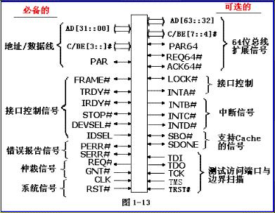
System signal
CLK IN:System clock signalProvides timing for all PCI transfers and is an input signal for all PCI devices. The frequency can be up to 33MHz/66MHz, which is also called the operating frequency of PCI.
RST# IN:Reset signal.Used to force all PCI-specific registers, sequencers, and signals to their initial state.
2. Address and data signals
AD[31::00]T/S:Address, data multiplexed signal. The transfer of addresses and data on the PCI bus must be performed during the FRAME# valid period. When the first clock is valid when FRAME# is active, the signal on AD[31::00] is the address signal, which is called the address period; when IRDY# and TRDY# are both active, the signal on AD[31::00] is The data signal is called the data period. A PCI bus transfer cycle consists of an address period followed by one or more data periods.
C/BE[3::0]# T/S:Bus commands and bytes allow multiplexing of signals. In the address period, these four lines transmit time bus commands; during the data period, they transmit the time byte enable signal, which is used to specify 4 data bytes on the AD[31::00] line during the data period. Which bytes are valid data for transmission.
PAR T/S:Parity signal. It performs parity check by AD[31::00] and C/BE[3::0]. The master drives PAR for address cycles and write data cycles, and the slave drives PAR for read data cycles.
3. Interface control signal
FRAME# S/T/S:Frame period signal, driven by the master device. Represents the start and duration of a bus transfer. When FRAME# is valid, it indicates the start of bus transmission; during its valid period, the address is transmitted first, and then the data is transmitted; when FRAME# is revoked, the bus transmission is predicted to end, and the data transmission of the last data period is performed when IRDY# is valid. .
IRDY# S/T/S:Master device ready signal. IRDY# should be used in conjunction with TRDY#. When both are valid, the data can be transmitted. Otherwise, it is not ready for two to enter the waiting period. During the write cycle, when the signal is valid, it indicates that the data has been submitted by the master device to the AD[31::00] line; during the read cycle, when the signal is valid, it indicates that the master device is ready to receive data.
TRDY# S/T/S:Ready signal from device (selected device). Similarly, TRDY# should be used in conjunction with IRDY#. Only when both are valid, data can be transmitted.
STOP# S/T/S:The slave device requires the master device to stop the signal of the current data transmission.. Obviously, this signal should be sent by the slave device.
LOCK# S/T/S:Lock signal. The exclusive use of the lock signal LOCK# for exclusive access to a device that may require multiple bus transfer cycles to complete. For example, if a device has its own memory, it must be able to lock in order to achieve full exclusive access to the memory. That is, the operation of this device is exclusive.
IDSEL IN:Initialize the device selection signal. Used as a chip select signal during parameter configuration read/write transfers.
DEVSEL# S/T/S:Device selection signal. This signal is issued by the slave when it recognizes the address. When it is valid, it indicates that a certain device on the bus has been selected and is the slave that is currently accessed.
4. Arbitration signal (only for bus master)
REQ# T/S:Bus occupancy request signal. This signal effectively indicates that the device that is driving it requires the use of a bus. It is a point-to-point signal line and any master device has its own REQ# signal.
GNT# T/S:Bus occupancy enable signal. This signal is valid, indicating that the request to apply for the device occupying the bus has been obtained.
5. Error report signal
PERR# S/T/S:Data parity error report signal. A device can report a PERR# only after responding to the device selection signal (DEVSEL#) and completing the data period.
SERR# O/D:System error reporting signal. Used as reporting address parity errors, data parity errors in special command sequences, and other system errors that can cause catastrophic consequences. It can be sent by any device.
6. Interrupt signal In the PCI bus, interrupts are optional and do not have to be.
INTA# O/D:Used to request an interrupt.
INTB# O/D、INTC# O/D、INTD# O/D:Used to request an interrupt, only meaningful for multifunction devices. The so-called multi-function device refers to the concentration of several independent functions in one device. The connection between each function and the interrupt line is arbitrary without any additional restrictions.
7. Other optional signals
(1) Cache support signals: SBO# IN/OUT, SDONE IN/OUT
(2) 64-bit bus extension signal: REQ64# S/T/S, ACK65# S/T/S、AD[63::32]T/S、C/BE[7::4]#T/S、PAR64 T/S。
(3) Test access port/boundary scan signals: TCK IN, TDI IN, TDO OUT, TMS IN, TRST# IN.
9054 feature description
9054Introduction:
The main function of PCI9054 is to realize data communication between PCI bus and local bus (generally Harvard structure). There are three kinds of data transmission modes: main mode, slave mode and DMA mode.
The PCI9054 chip is mainly composed of two data FIFO channels, internal registers, EEPROM and control circuits. The two channels are DMA0 and DMA1 respectively, and their functions are basically the same, and DMA0 can also transmit command commands.
PCI9054 has three working modes: M, J, C
M mode, a non-multiplexed interface directly prepared for Motorola's MPC850 and MPC860;
C mode, address, data lines are not multiplexed;
J mode, address data line multiplexing.
Due to MThe mode is relatively small, JMode control is more complicated, generally use Cmode.
PIN definition:
All modes
AD[31:0] (Address and Data) address and clock multiplexing, first of all an address segment, followed by one or more data segments, support burst mode read and write;
The C/BE[3:0]# (Bus Command and Byte Enables) bus command and data enable multiplexing pins are used as bus commands when AD is the address line and as data when AD is the data line.
When DEVSEL# (Device Select) is valid, it indicates that the current device is selected as the input port;
FRAME# (Cyclone Frame) is driven by the master device to indicate that the current device has started to access and the bus starts transmitting data. Valid: Transfer data. Invalid: complete the transmission of the last data;
GNT#(Grant) is used to indicate that the currently accessed device has been accepted.
IDSL (Initialization Device Select) is used as a chip select signal when the configuration register is read or written;
INTA# (Interrupt A) PCI interrupt request;
IRDY# (Initiator Ready) indicates that the current data is valid and can be completed and completed.
LOCK#(Lock) prompts for automatic operation and requires several clocks to complete the operation;
PAR (Parity) is the base parity of the AD and C/BE two-part bus. When the address is transmitted, the PAR is stable for one clock cycle after the address is transmitted. For data segments, PAR is stable for one clock cycle after IRDY# or TRDY# is active. Once the PAR data is valid, it will remain valid until the end of the current data or address segment transmission;
PCLK (Clock) system clock, 9054 works at 33MHz;
PERR# (Parity Error) is used to report parity errors, excluding special periods;
PME# (Power Management Event) wakeup interrupt;
REQ# (Request) request signal to inform the bus decider that the current device must use the bus;
RST# (Reset) system reset;
SERR# (System Error) is used to report parity errors and other system errors for special periods;
STOP#(Stop) requires the main system to stop the data transmission of the current device;
TRAY# (Target Ready) target device is ready to transfer current data;
BIGEND#(Big Endian Select)
CCS# (Configuration Register Select) low effective chip select signal;
EECS (Serial EEPROM Chip Select) selects the serial EEPROM;
EEDI/DDEO (Serial EEPROM Data In/ Serial EEPROM Data Out) controls serial EEPROM read and write data;
EESK (Serial Data Clock) EEPROM read and write clock;
ENUM# (Enumeration) burst output, used to indicate that an adapter using the PCI9054 chip has just been added or removed from a CPI bus channel;
Local clock input of LCLK (Local Processor Clock);
LEDon/LEDin LED control;
LFRAME# (PCI Buffered FRAME# Signal) indicates the status of the PCI bus;
LINT# (Local Interrupt) Local bus interrupt. Input to 9054, active low, triggering a PCI interrupt. As an output, wait until a trigger occurs;
LRESETo# (Local Bus Reset Out) When the PCI9054 chip is reset, this pin can be used to drive the RESET# signal of other chips;
MDREQ#/MDPAF/EOT#
MODE[1:0] (Bus Mode) 11: M mode; 10: J mode; 01: Reserved; 00: C mode;
TEST (Test Pin) chip detects the pin, the high is the detection, the low is the work, and the low is usually low;
USERi/BACK0#/LLOCKi# Multiplexed Pins
USERo/DREQ0#/LLOCKo# Multiplexed Pins
VDD power supply
VSS ground
C mode:
ADS# (Address Strobe) indicates that the address is valid and the bus has new equipment access;
BLAST# (Burst Last) This signal is controlled by the local bus and represents the transmission of the last character;
BREQi (Bus Request In) local bus control, data is input from the local bus;
BREQo (Bus Request Out) PCI bus control, data is output from the PCI bus;
BTERM# (Burst Terminate) is used as an input to indicate the end of the current burst operation, to start reading and writing the next burst address, and to be used with the programmable wait state generator inside the PCI9054. As an output, used with READY# to interrupt the current burst operation and start the next burst operation address cycle;
DP[3:0] (Data Parity) parity data;
LA[31:2] (Address Bus) address bus;
LBE[3:0]# (Byte Enable) control data is valid, different modes have different control methods;
LD[31:0] (Data Bus) data bus;
The LHOLD (Hold Request) transmission requires the use of a local bus. After the local bus decides to allocate to the current device, the decider sends LHOLDA signal feedback.
LHOLDA (Hold Request) feedback signal;
LSERR# (System Error Interrupt Output) system error interrupt;
LW/R# (Write/?Read) low level read, high level write;
READY#(Ready Input/Output) means that the data is ready and valid regardless of the master or slave mode;
WAIT# (Wait Input/Output) is used as an input to control the PCI9054 insertion wait state. As an output, the PCI9054 is in the Ready state.
J mode:
ADS# (Address Strobe) indicates that the address is valid and the bus has new equipment access;
ALE (Address Latch Enable) address is valid when transmitting, and invalid when data is transmitted;
BLAST# (Burst Last) This signal is controlled by the local bus and represents the transmission of the last character;
BREQi (Bus Request In) local bus control, data is input from the local bus;
BREQo (Bus Request Out) PCI bus control, data is output from the PCI bus;
BTERM# (Burst Terminate) is used as an input to indicate the end of the current burst operation, to start reading and writing the next burst address, and to be used with the programmable wait state generator inside the PCI9054. As an output, used with READY# to interrupt the current burst operation and start the next burst operation address cycle;
DEN# (Data Enable) is used in conjunction with DT/R# to control the data transceiver connected to the local bus;
DP[3:0] (Data Parity) parity data;
DT/R# (Data Transmit/Receive) is used in conjunction with DEN#. When valid, PCI9054 receives data.
LA[28:2] (Local Address Bus) local bus address;
LAD[31:0] (Address/Data Bus) Address Period: This bus contains the upper 30 bits of the physical address bus. Data cycle: the bus transmits 32-bit data;
LBE[3:0]# (Byte Enable) control data is valid, different modes have different control methods;
The LHOLD (Hold Request) transmission requires the use of a local bus. After the local bus decides to allocate to the current device, the decider sends LHOLDA signal feedback.
LHOLDA (Hold Request) feedback signal;
LSERR# (System Error Interrupt Output) system error interrupt;
LW/R# (Write/Read) low level read, high level write;
READY#(Ready Input/Output) means that the data is ready and valid regardless of the master or slave mode;
WAIT# (Wait Input/Output) is used as an input to control the PCI9054 insertion wait state. As an output, the PCI9054 is in the Ready state.Call my teacher's artificial intelligence tutorial!this link

Intelligent Recommendation

Use python to crawl the cover picture of Huya anchor live broadcast (scrapy)
Purpose: Use Scrapy framework to crawl the cover image of Huya anchor live broadcast Scrapy (install the Scrapy framework through pip pip install Scrapy) and Python3.x installation tutorial can find t...

Learning Record - ES6 Modularity and Node (2020-12-10)
1, what is Node? 2, Node and Java / PHP difference? 2.1, node.js and java distinction: 2.2, Node.js and PHP distinction: 3, ES6 modularization (Quote, extracted from) 3.1, Export usage: If you want to...
MAX5468 digital potentiometer
Regarding the use of the MAX5468 digital potentiometer, the digital potentiometer can avoid manual control resistance changes to control the volume. This digital potentiometer has 6 pins. The most pro...
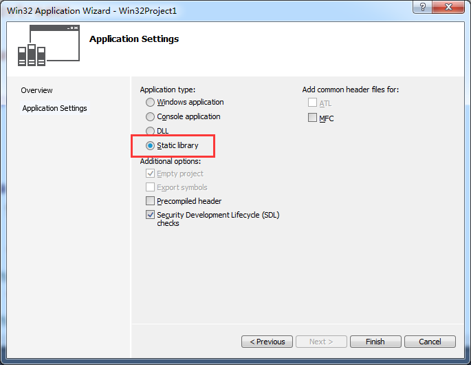
Application of creating and using static libraries
Highly recommended to watchMicrosoft official documents。 Static library Using static libraries (.lib files) is an excellent way to reuse code. Rather than re-implementing the same routine requires one...
More Recommendation
Android develops a simple player based on ffmpeg - basics
Audio and video basics Video file format For video, common file formats are: .mov, .avi, .mpg, .vob, .mkv, .rm, .rmvb, and more. The file format usually appears as the suffix of the file when it is st...

Some problems with shared folders between win8.1 and Ubuntu virtual machine on VirtualBox
VirtualBox: Select the virtual machine--settings--shared folder--add shared folder--path--name--fixed allocation--(automatically mount (this will mount the folder to the /media/ directory) Start Ubunt...
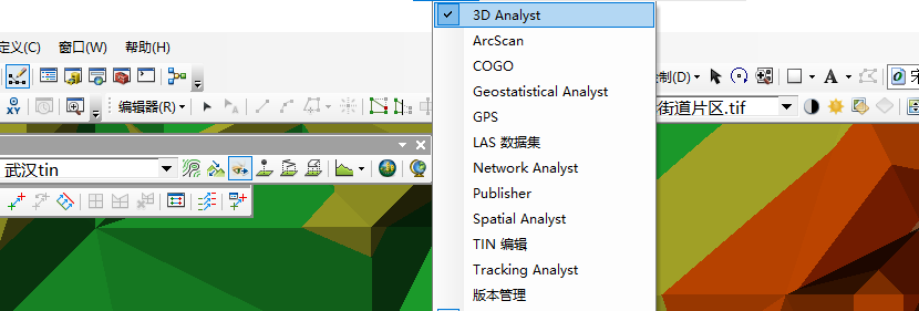
GIS Sight Analysis
Very simple very simple and the most basic part! Emphasis: the target data is TIN data! ! ! 1. Bring up the 3D Analyst toolbar 2. Specify the layer for analysis 3. Create line of sight and set paramet...
ESP-IDF installation Configure Edible Tutorial (Example of Windows System)
Article catalog Foreword First, pre-preparation Second, environmental configuration 1.python installation 2.git installation Third, ESP-IDF installation Fourth, other Five, conclusion Foreword Xu Xiao...