The design of the asynchronous FIFO
tags: Digital IC FPGA development
Async_fifo classic framework:
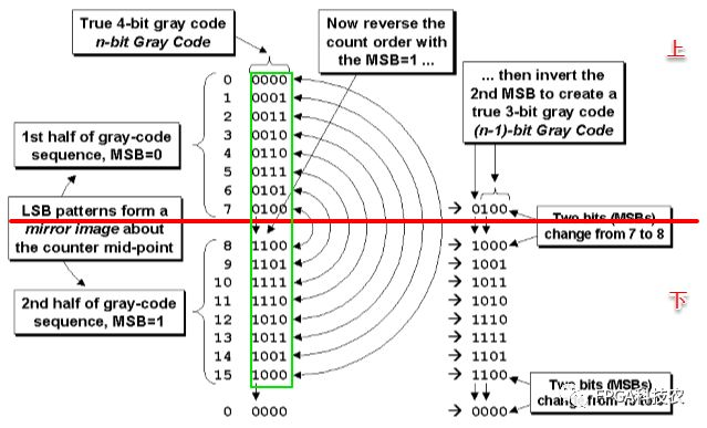
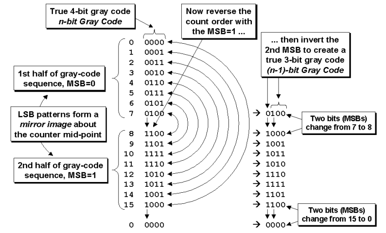
The address of the empty judgment is converted by Gray code, and the output is shot
The high two bit is the opposite, and the other bit is the same: the same:
Both are equal to empty;
The extension of RAM is as follows:
dual_ports_sram:
module dual_port_ram #(parameter WIDTH= 8,parameter DEPTH = 16,parameter ADDR=$clog2(DEPTH))
    (input wclk,
    input rclk,
    input [WIDTH-1:0]wdata,
    input wenc,
    input renc,
    input [ADDR-1:0]waddr,
    input [ADDR-1:0]raddr,
    output reg [WIDTH-1:0]rdata
);
/*----------sram----------*/
reg [WIDTH-1:0]ram[DEPTH-1:0] ;

/*------write operation -------*/
always @(posedge wclk) begin
    if(wenc)
        ram[waddr] <= wdata;
end

/*------read operation -------*/
always @(posedge rclk ) begin
    if(renc)
        rdata <= ram[raddr];
end

endmodule //dual_port_ram
async_fifo.v
//async_fifo
`timescale 1ns/1ps

module async_fifo #(parameter WIDTH=8,parameter DEPTH=16,parameter ADDR_BIT = $clog2(DEPTH);)(
    input rrstn,wrstn,
    input wclk,rclk,
    input wenc,renc,
    input [WIDTH-1:0]wdata,
    output wire [WIDTH-1:0]rdata,  //
    output wire full,
    output wire empty
);
/*---------address declare-------------*/

reg [ADDR_BIT:0]waddr;
reg [ADDR_BIT:0]raddr;
/*------------write addr---------------*/
always@(posedge wclk or negedge wrstn)begin
    if(!wrstn)
        waddr <= 'b0;
    else if(wenc && ~full)
        waddr <= waddr + 1'b1;
    else
        waddr <= waddr;
end
/*------------read addr---------------*/
always@(posedge rclk or negedge rrstn)begin
    if(!rrstn)
        raddr <= 'b0;
    else if(renc && ~empty)
        raddr <= raddr +1'b1;
    else
        raddr <= raddr;
end
/*------------W2R bin to gray---------------*/
wire [WIDTH:0]r_gaddr ;
wire [WIDTH:0]w_gaddr ;

assign r_gaddr = raddr ^ (raddr>>1);  //bin to gray code;for
assign w_gaddr = waddr ^ (waddr>>1);

reg [ADDR_BIT:0]w_gaddr_reg;  //Hit one beat in the write clock domain
always@(posedge wclk or negedge wrstn)begin
    if(!wrstn)
        w_gaddr_reg <= 'd0;
    else
        w_gaddr_reg <= w_gaddr;
end

reg [ADDR_BIT:0]r_gaddr_reg;//Hit one beat in the read clock domain
always @(posedge rclk or negedge rrstn) begin
    if(!rrstn)
        r_gaddr_reg <= 'd0;
    else
        r_gaddr_reg <= r_gaddr;
end
/*------------After Clock Domain Crossings, hit two beats to make empty judgment----------------*/
reg [ADDR_BIT:0]addr_w2r_t;
reg [ADDR_BIT:0]addr_w2r;
always@(posedge rclk or negedge rrstn)begin
    if(!rrstn)begin
        addr_w2r_t <= 'd0;
        addr_w2r   <= 'd0;
        end
    else begin
        addr_w2r_t <= w_gaddr_reg;  //Send the address generated by the write clock domain into the read clock domain
        addr_w2r   <= addr_r2w_t;
    end
end
/*------------After Clock Domain Crossings, hit two beats to make full judgment---------------*/
reg [ADDR_BIT:0]addr_r2w_t;
reg [ADDR_BIT:0]addr_r2w;
always@(posedge wclk or negedge wrstn)begin
    if(!wrstn)begin
        addr_r2w_t <= 'd0;
        addr_r2w   <= 'd0;
        end
    else begin
        addr_r2w_t <= r_gaddr_reg;  //
        addr_r2w   <= addr_r2w_t;
    end
end
assign empty = (addr_r2w == addr_w2r);
assign full  = (addr_r2w == {~addr_w2r[ADDR_BIT:ADDR_BIT-1],addr_w2r[ADDR_BIT-2:0]});
/*------------sram instanse---------------*/
dual_port_ram #(.DEPTH(DEPTH),
                .WIDTH(WIDTH),
                .ADDR(ADDR_BIT))
dual_port_ram_ins(
        .wclk(wclk),
        .rclk(rclk),
        .wenc(wenc && ~full),
        .renc(renc && ~empty),
        .wdata(wdata),
        .rdata(rdata),
        .waddr(waddr[ADDR_BIT-1:0]),  //-1,,SRAM
        .raddr(raddr[ADDR_BIT-1:0])
);


endmodule //async_fifo
Intelligent Recommendation
Verilog design of asynchronous FIFO
1. The concept of asynchronous FIFO Asynchronous FIFO uses different clocks for reading and writing. The asynchronous FIFO is used to transmit data in different clock domains, and is mainly used to tr...

Design of asynchronous fifo (two)
This article continues from the previous article, first look at the overall block diagram of asynchronous fifo design: There will be 6 small modules in this design: 1. The fifo.v module is the top-lev...
Synchronous and asynchronous FIFO design
Synchronous FIFO design Signal list CLK: FIFO operation clock WR_EN: FIFO write enable, in the case of WR_EN is effective, the rising edge collects WDATA data. WDATA: FIFO write data. Full: FIFO is fu...
Asynchronous FIFO Design (4)
This article is mainly realized by the Verilog code of the last article, and now posts the code:...
Asynchronous FIFO design code
The RTL code of asynchronous FIFO mainly contains 6 modules: (1)fifo_top.v、(2)fifo_mem.v、(3)sync_w2r.v、 (4)sync_r2w.v、(5)wptr_full.v、(6)rptr_empty.v (1)fifo_top.v:Top-level module, mainly instantiates...
More Recommendation
FIFO series (three): fifo and gray code and asynchronous fifo design
This series is divided into the following parts: 1. FIFO depth calculation 2. Synchronous fifo design 3. Design of fifo and gray code and asynchronous fifo The plan has been updated in three stages, t...
Design of asynchronous FIFO based on verilog
WeChat public account "FPGA Technology Room" From the hardware point of view, the FIFO studied in this article is a piece of data memory. It has two ports, one for writing data, that is, sto...
Reading notes------------------Asynchronous FIFO design
FIFO is often used to process multi-bit width data across clock domains. In actual use, we generally instantiate the IP core of the FIFO directly, and realize the control of the FIFO by calling the IP...

RTL Design (5) - Asynchronous FIFO
Asynchronous FIFO Introduction to FIFO Asynchronous FIFO Full Test Asynchronous FIFO minimum depth Asynchronous FIFO instance operation result Introduction to FIFO FIFO (First In First Out is an advan...