Altium Designer's method to remove dead copper (rule check hint: isolated copper)
tags: Altium Designer AD Dead copper isolated copper PCB
In the PCB rule check in AD, when the isolated copper: split plane (dgnd) on ground, dead copper delected. copper area is: 2.5e2 sq. mils error appears, there is dead copper or no network connection.

Here is only an effective method of processing
Approach:
1. Find the location of the dead copper first:
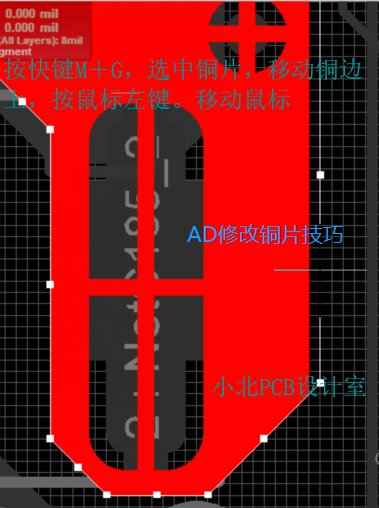
1. When you don’t know the position of the dead copper (when the DRC check is wrong, the position will be displayed when the mouse is placed in the wrong place), first reduce the PCB, place the mouse on the PCB, and move it so that the isolated copper...has dead copper in the upper left corner of the PCB Wrong prompt

2. Press Shift + V again, the following window will appear, left click to select Select

3. Edit -> Jump -> Selection

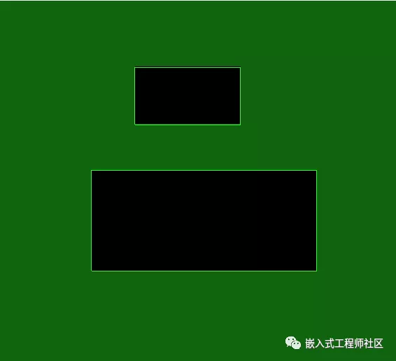
4. At this time, zoom in to see the dead copper, which is marked in green

5. Re-check the rules after removal.
Intelligent Recommendation
Altium Designer modifies copper tips
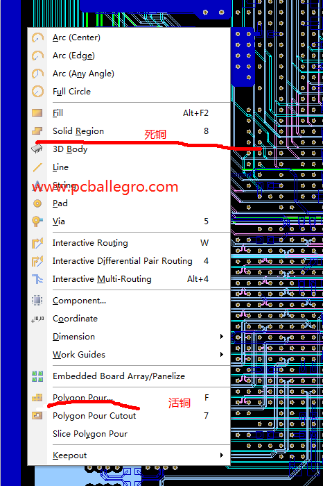
When applying/laying copper, it is best to lay it on the 5mil grid. Why do you want to press 5 points? Because at 5 grids, we can make changes to the copper and capture. In ad, there are two kinds of ...

Altium Designer circular, oval copper
The key: Check the circle drawn, Tools -> Covert -> elements selected from the creation of regional 1, with the copy or drawing a circle or ellipse Videos manner. 2, for example, an upper...
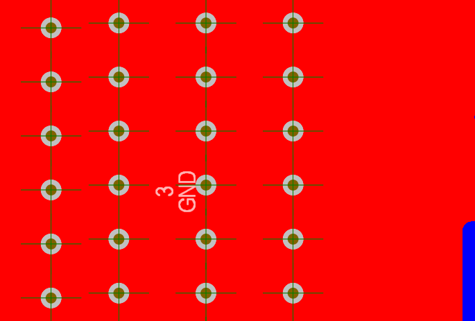
isolated copper:split plane(dgnd) on ground,dead copper delected.copper area is: 2.5e2 sq.mils
This kind of error prompt may appear when the AD is inspected, don't panic, it is very simple to solve: Generally, there is a dead copper, you need to go What you have to do is positioning a tip, you ...
[Raiders] Use Altium Designer software to dig copper after laying copper
After using Altium Designer to lay copper, there will always be unsatisfactory places, or places that need to be slightly modified, then you need to modify it by laying copper and digging holes. Use s...

How to perform copper pour and mesh copper pour in Altium Designer?
Author: Li Chuang This article hopes to explain the following three questions to readers: 1. How to carry out copper pour in Altium Designer? 2. How to perform mesh copper pour in Altium Designer? 3. ...
More Recommendation
Altuim designer how to turn live copper into dead copper
Altuim designer how to turn live copper into dead copper Altuim Designer by PCB High Speed Design Solution, Xiaobei Design altuim designer How to turn live copper into dead copper altuim designer Th...
Allegro-Remove copper skin void
After placing voids on the copper skin How can this hollowed out area be deleted? Solution: Enter shape edit mode Click on the menu bar Shape—Manual Void/Cavity—Delete Only check void/cavi...
Altium Designer 16 Modifying the Copper Rules
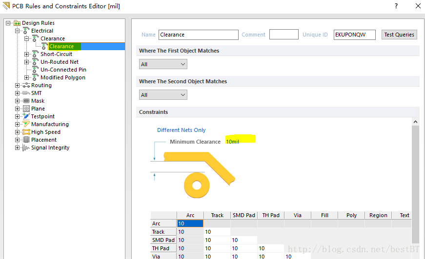
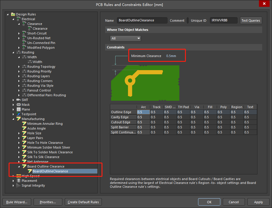
Transfer from When I made my first board, I didn't pay attention to the problem of spacing between copper and the network. The software gives me 6mils according to the default spacing between differen...

Altium Designer copper regular spacing provided
1. Create a new spacing rules and change the name 2. Click the above "where the first object matches" box below the senior side, click "Query Builder" "Condition Type / operat...
Pitch copper plate frame is provided with Altium
PCB proofing manufacturers are required and the distance between the copper plate and frame, just beginning to learn Altium drawing board, I was reduced copper within the manual, and now think of it, ...