(Based on STM32F407) Learn STM32 SW and JTAG debug and download circuit design
Article Directory
I. Introduction
The development of STM32 circuit boards must understand the design of the STM32 download and debug circuit, in order to ensure the subsequent download and debugging of the STM32 development board.
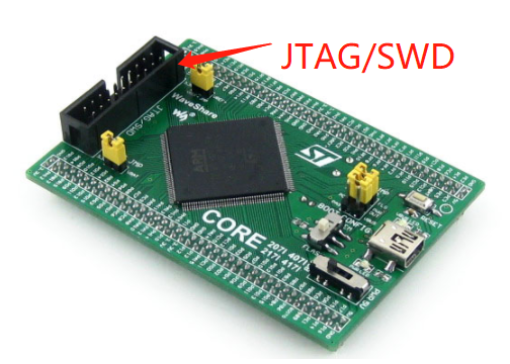
The picture below is the standard JTAG/SWD download and debug connector (taken from Micro Snow Electronics):
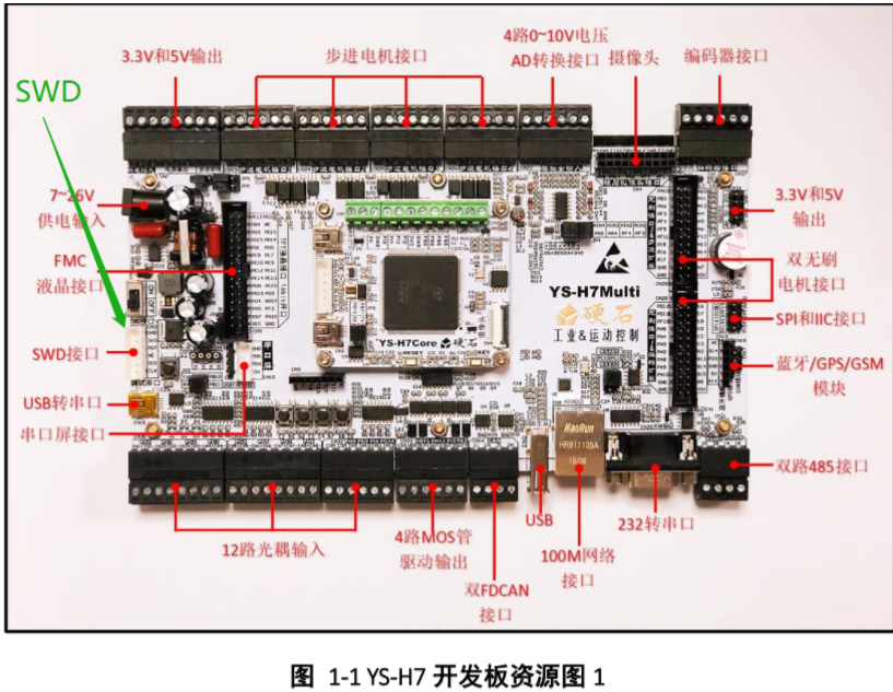
There are also some manufacturers that only retain the SWD interface. The following picture is a non-standard connector (taken from Hard Rock Technology):
At present, the SWD interface is most commonly used. At work, I also only use the SWD interface. This time the note recording is also based on the theme of SWD.
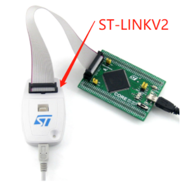
The SWD interface needs to be used with ST-LINK. The price of ST-LINK is much cheaper than that of J-LINK.
2. SWD circuit design
SWD only needs 4 wires to complete the programming and debugging of the program. With ST-LINK, the price is cheap, and it is the best combination for STM32 development at present.
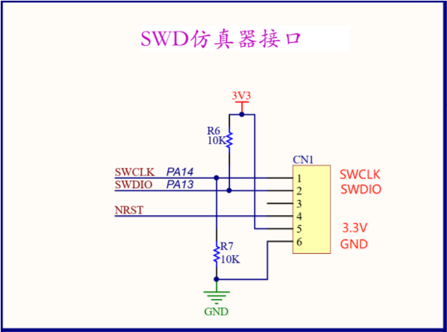
The following picture is taken from the F4 development board of Hard Rock Technology:
There is no problem in applying the circuit in the above picture directly to your own project. However, it is better to understand the following two questions:
1. Why does SWCLK need to be pulled down to GND through a 10K resistor?
2. Why does SWDIO need to be pulled up to 3.3V through a 10K resistor?
3. Hardware design-SWCLK and SWDIO
Now let's understand the reasons for SWCLK pull-down and SWDIO pull-up.
Refer to "STM32F4xx Chinese Reference Manual" page 1247, Chapter 33-Debugging Support.
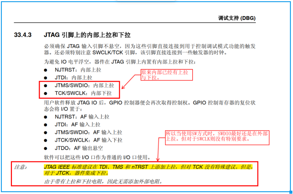
As you can see from the picture above,In fact, SWDIO and SWCLK already have pull-ups and pull-downs.。
SWCLK/TCK, there is no special recommendation on the circuit board to pull down further
Next, check page 1251 of "STM32F4xx Chinese Reference Manual":
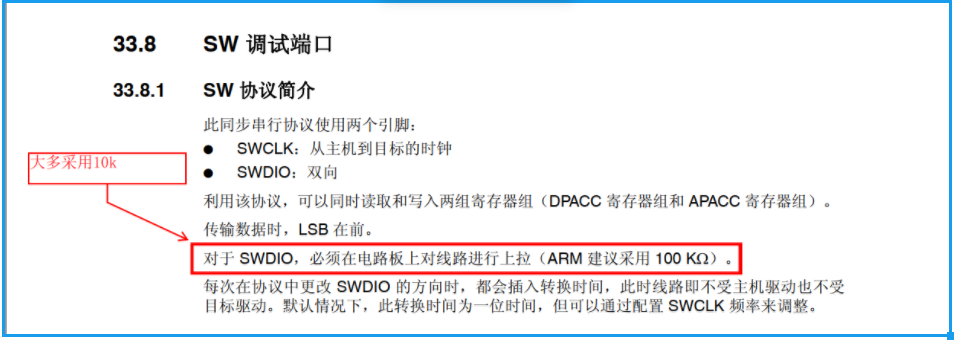
As you can see from the figure above, ARM officially recommends using a 100k resistor for pull-up on SWDIO. However, most people just use 10k pull-ups. I have tried these two schemes personally, and found no difference.
SWDIO, there is a pull-up inside the chip, but it must be pulled up again on the circuit board (100k or 10k resistance)
SWCLK has been pulled down inside the chip, and there is no special requirement for further pulling down on the circuit board.
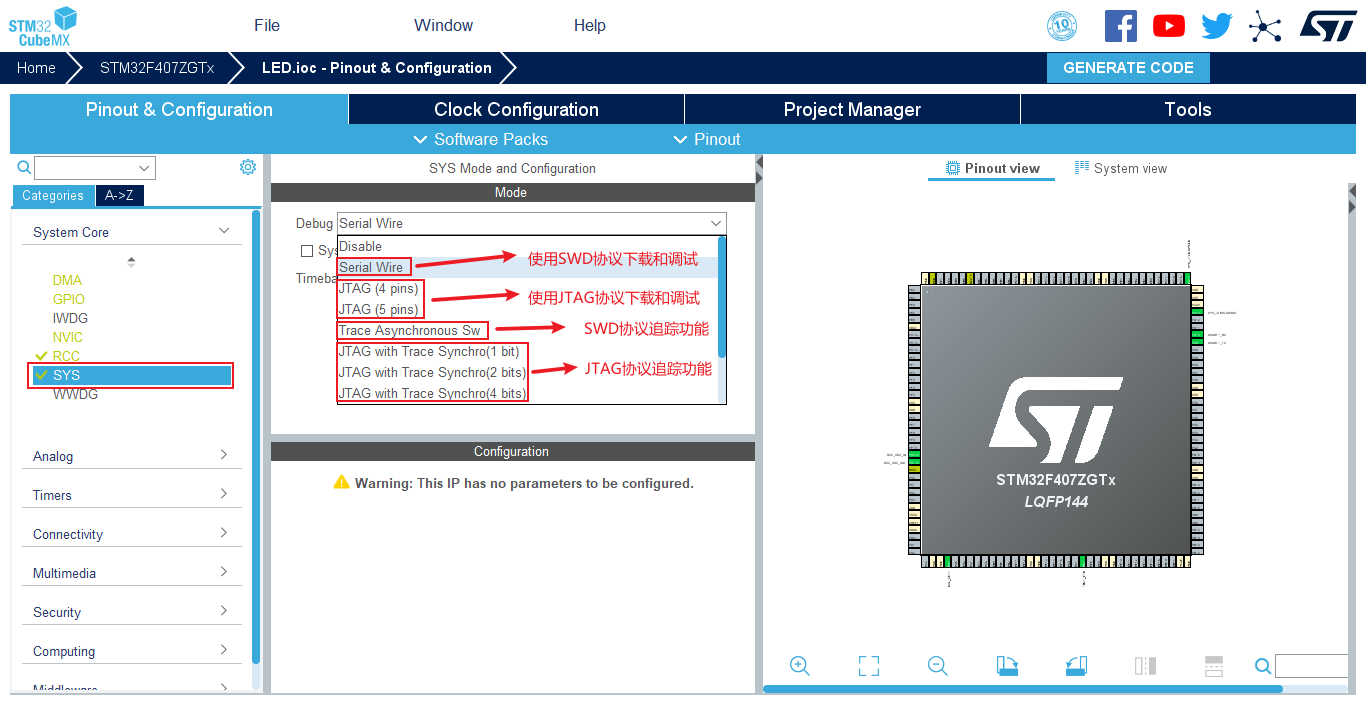
Fourth, the code-STM32CubeMX
After understanding the hardware design of the SWD method, then look at the code configuration (Important)!
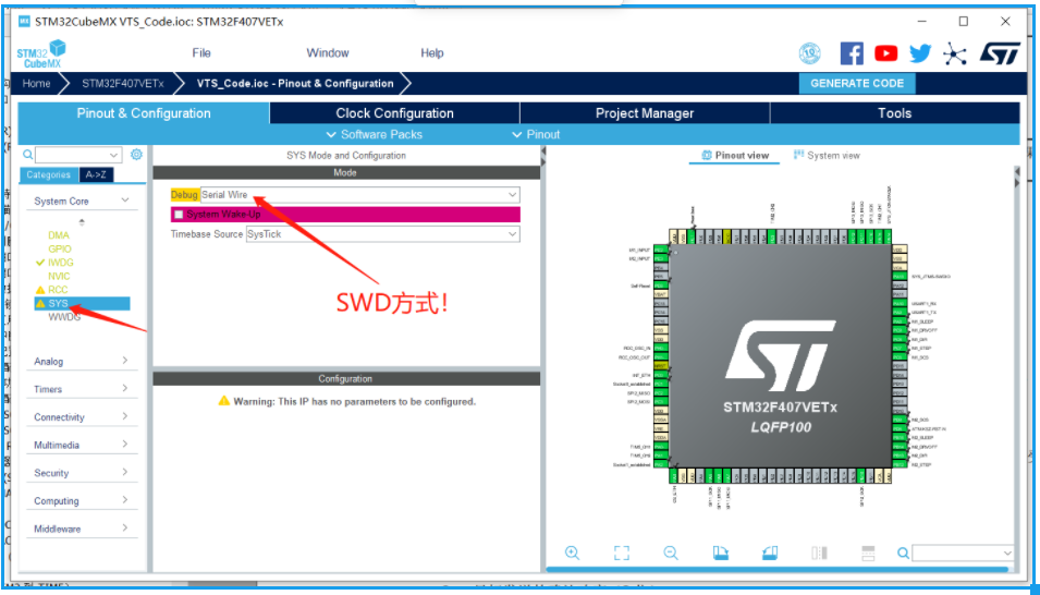
As shown in the figure above, Debug needs to select Serial Wire (SWD mode).As for why do I need to configure Serial Wire? The reason is that all GPIO ports of STM32 have multiplexing functions. Among them, PA13 and PA14 have two functions.
As shown in the figure below, PA13 can be JTMS or SWDIO. STM32 defaults to JTAG mode, so PA13 defaults to JTMS, not SWDIO.
In the Debug column, after selecting Serial Wire (SWD mode), PA13 is SWDIO and PA14 is SWCLK. Then PA15, PB3, PB are just ordinary GPIO.
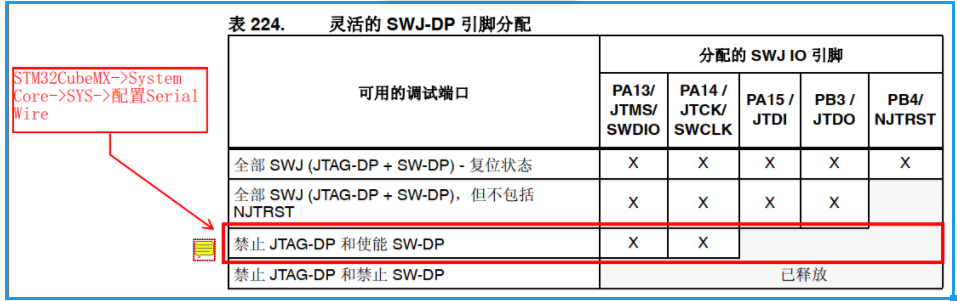
In short, if you choose Serial Wire, it is equivalent to "disable JTAG-DP and enable SW-DP", that is, turn off JTAG and turn on SWD at the same time.
Five, the pit of ST-LINK V2
The combination of ST-LINK V2 + SWD is not perfect. There are also some pits, refer to the following URL:
The pit of ST-LINK V2
Intelligent Recommendation
STM32 ~ JTAG, SWD and serial download problems
Recently, a project to use STM32, PCB layout in order to make it convenient to change some of the pins, taking up PA15 and PB3 JTAG interface, so what you want to disable JTAG, SWD mode using download...
Connect the SW port of JLINK to the SW port of JTAG
Main content: Connect the SW port of JLINK to the SW port of JTAG the reason: step 1 Find the circuit diagram of the JTAG interfaceSW: Four wires of CLK+SWD+VCC+GND Step 2 Connect the four wires of th...
Design of STM32-based balance car robot-hardware circuit design
Today I will share the hardware circuit design of a self-balancing car robot with STM32F103 as the main control. (Pro-test is completely available without any problems) Circuit schematic diagram: The ...
Download stm32 circuit
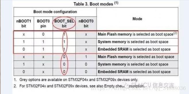
As can be seen from the figure, there are two ways to start, the first activation mode is determined by using a physical pin and BOOT0 Nboot1, Boot_Sel option bit; second only Boot_Sel, Nboot1, Nboot0...
STM32CubeMX SYS SW JTAG configuration
STM32 debug interface configuration 1. Select the download and debug interface in STM32CubeMX There are SW and JTAG protocol options in the SYS option bar of STM32CubeMX. Users can select the correspo...
More Recommendation
[STM32] Interrupt switch point lamp based on STM32F407
contents First, interruption introduction What is the interrupt? 2. The role of interrupt 3. Interrupt type and priority Second, interruption light New project 2. Write code 3. Burning verification Th...
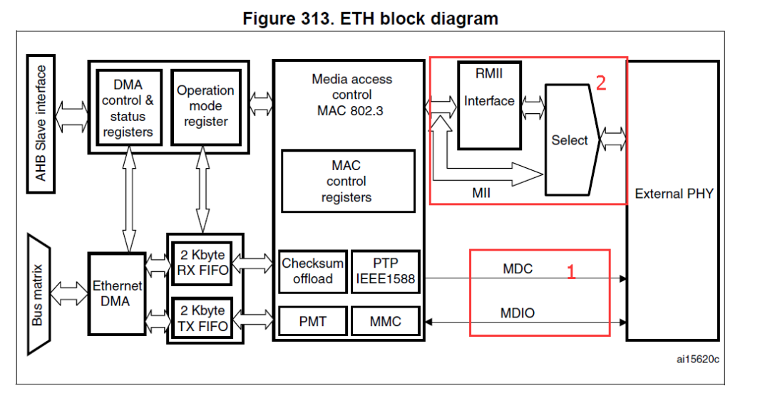
STM32 network circuit design
table of Contents 01, MII interface solution 02, RMII interface solution 2.1, external crystal oscillator (2 crystal oscillators) 2.2, external crystal oscillator (1 crystal oscillator) 2.3. Need a po...

STM32 circuit design explanation
STM32 hardware circuit diagram problem STM32 VBAT pin STM32 VBAT pin 1, VBAT: When using a battery or other power supply to the VBAT feet, when VDD is powered off, the contents of the backup register ...
Chapter 1 Circuit Design and Production Process Based on STM32 Cyber
This note is mainly to learn the circuit design, you can make a board! ! ! All notebooks of all notes come from the B station: The information of this video is here: Data package latest link Link: htt...
Debugging and download based on JTAG for ESP32-C3
Foreword In the first chapter"Construction of ESP32C3 development environment based on VSCODE"After that, Xiaobian believes that most readers can easily set the ESP32-C3 development environm...