Stm32f4 adc use
forward from:
Stm32 related articles can refer to the above URL
Chapter 30 ADC - Voltage Acquisition
A full set of 200 video tutorials and 1000 pages of PDF tutorials are available for download on the Bing Fire Forum:www.firebbs.cn
Wildfire video tutorial Youku watch URL: http://i.youku.com/firege
References in this chapter: "STM32F4xx Chinese Reference Manual" ADC chapter.
When you read this chapter, you can read it together with the ADC chapter of the STM32F4xx Chinese Reference Manual. The effect will be better, especially when it comes to register description.
30.1 ADC Introduction
The STM32F429IGT6 has three ADCs, each with 12, 10, 8, and 6 bits, each with 16 external channels. There are also two internal ADC sources and a VBAT channel attached to ADC1. The ADC has an independent mode, a dual mode, and a triple mode, and almost all of the different AD conversion requirements are available. The ADC is very powerful, and we analyze the function of each part in the functional block diagram.
30.2 ADC functional block diagram analysis
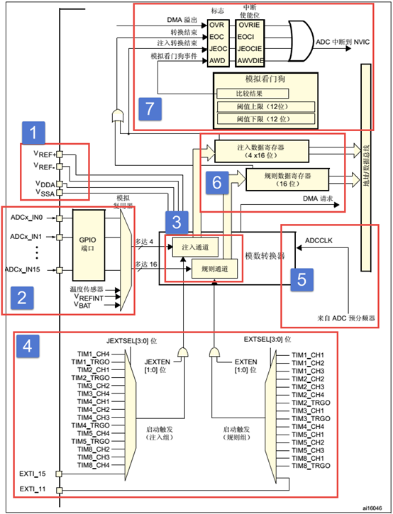
Figure 01 Single ADC Functional Block Diagram
Mastering the functional block diagram of the ADC, you can have an overall understanding of the ADC, and you can do it in the programming, you will not know it. The block diagram explains the way from left to right, collecting data with the ADC, converting the data, and transmitting the data in the same direction.
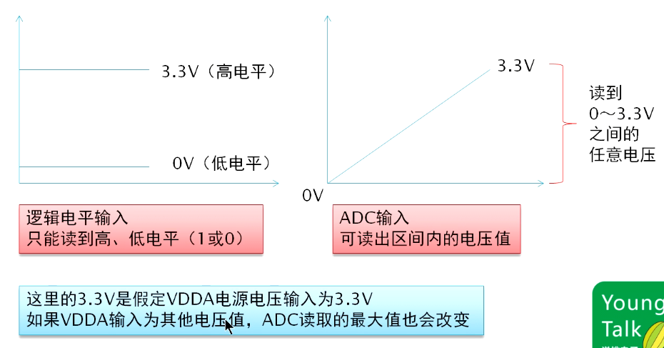
1. 1 voltage input range
The ADC input range is: VREF- ≤ VIN ≤ VREF+. It is determined by four external pins: VREF-, VREF+, VDDA, VSSA.
When designing the schematic, we generally ground VSSA and VREF-, connect VREF+ and VDDA to 3V3, and get the input voltage range of the ADC: 0~3.3V.
If we want to widen the input voltage range and go to test a negative voltage or a higher positive voltage, we can add a voltage conditioning circuit externally to boost or step down the voltage to be converted to 0~3.3V. The ADC can be measured.
2. 2 input channels
After we determine the ADC input voltage, how is the voltage input to the ADC? Here we introduce the concept of channel, STM32 ADC up to 19 channels, of which the external 16 channels are ADCx_IN0, ADCx_IN1...ADCx_IN5 in the block diagram. These 16 channels correspond to different IO ports, and which IO port can be queried from the manual. Among them, ADC1/2/3 also has internal channels: ADC1 channel ADC1_IN16 is connected to internal VSS, channel ADC1_IN17 is connected to internal reference voltage VREFINT connection, channel ADC1_IN18 is connected to the chip internal temperature sensor or standby power supply VBAT. Channels 16, 17, and 18 of ADC2 and ADC3 are all connected to the internal VSS.
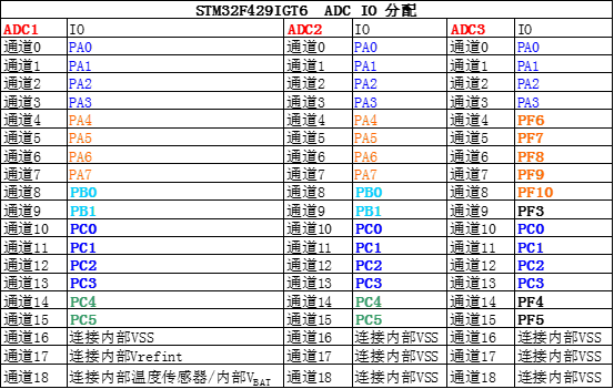
Figure 02 STM32F429IGT6 ADC Channel
The 16 external channels are divided into regular channels and injection channels during conversion. The regular channels have a maximum of 16 channels and the injection channel has a maximum of 4 channels. What is the difference between these two channels? When is it used?
Rule channel
Rule channel: As the name implies, the rule channel is very regular. We usually use this channel, or we should say that we use this channel. There is nothing special to pay attention to.
Injection channel
Injection can be understood as inserting, meaning of cutting the queue, is a channel of restlessness. It is a type of forced insertion to be converted when a regular channel is converted. If there is an injection channel in the regular channel conversion process, then the injection channel is first converted, and after the injection channel conversion is completed, it returns to the conversion process of the regular channel. This is very similar to the interrupt program, and it is the leader of restlessness. Therefore, the injection channel will only appear when the regular channel exists.
3. 3 conversion order
Rule sequence
There are three rule sequence registers, which are SQR3, SQR2, and SQR1. SQR3 controls the first to sixth transitions in the rule sequence. The corresponding bits are: SQ1[4:0]~SQ6[4:0], and the first conversion is bit 4:0 SQ1[4:0 ], if channel 16 wants to convert for the first time, then write 16 in SQ1[4:0]. SQR2 controls the 7th to 12th transitions in the rule sequence. The corresponding bits are: SQ7[4:0]~SQ12[4:0]. If channel 1 wants the 8th conversion, then SQ8[4:0] Write 1 to. SQR1 controls the 13th to 16th conversions in the rule sequence. The corresponding bits are: SQ13[4:0]~SQ16[4:0]. If channel 6 wants the 10th conversion, then SQ10[4:0] writes 6 can be. How many channels are used, which is determined by the bit L[3:0] of SQR1, and up to 16 channels.
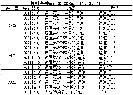
Figure 03 Rule Sequence Register
Injection sequence
There is only one injection sequence register JSQR, which supports up to 4 channels, and the specific number is determined by JL[2:0] of JSQR. If the value of JL is less than 4, the JSQR is not the same as the setting of SQR to determine the conversion order. The first conversion is not JSQR1[4:0], but JCQRx[4:0], x = (4-JL), The opposite of SQR. If JL=00 (1 conversion), then the order of conversion starts from JSQR4[4:0], not from JSQR1[4:0], so be careful not to make mistakes when programming. When JL is equal to 4, it is the same as SQR.

Figure 04 Injection Sequence Register
4. 4 trigger source
The channel is selected, the order of the conversion is also set, and then it is time to start the conversion. ADC conversion can be controlled by ADC control register 2: ADON bit of ADC_CR2, start conversion when writing 1, stop conversion when writing 0, this is the simplest and best understood control method to turn on ADC conversion, understand no Technical content.
In addition to this unobstructed control method, the ADC also supports external event trigger conversion, which includes internal timer triggering and external IO triggering. There are many trigger sources. Which trigger source is selected is controlled by the EXTSEL[2:0] and JEXTSEL[2:0] bits of ADC Control Register 2: ADC_CR2. EXTSEL[2:0] is used to select the trigger source of the regular channel, and JEXTSEL[2:0] is used to select the trigger source of the injection channel. After the trigger source is selected, whether the trigger source is to be activated or not is activated by the two bits of ADC control register 2: ADC_CR2, EXTTRIG and JEXTTRIG.
If the external trigger event is enabled, we can also control the trigger polarity by setting the ADC control register 2: ADC_CR2's EXTEN[1:0] and JEXTEN[1:0]. There are four states, namely: disable trigger Detection, rising edge detection, falling edge detection, and both rising and falling edges are detected.
5. 5 conversion time
ADC clock
ADC input clock ADC_CLK is divided by PCLK2, the maximum value is 36MHz, the typical value is 30MHz, the division factor is set by ADCPRE[1:0] of ADC general control register ADC_CCR, the set frequency division coefficient is 2, 4, 6 and 8, note that there is no divide by one. For STM32F429IGT6 we generally set PCLK2 = HCLK / 2 = 90MHz. So the program generally uses a divide by 4 or a divide by 6.
sampling time
The ADC requires several ADC_CLK cycles to sample the input voltage. The number of samples can be set by the SMP[2:0] bits in the ADC sample time registers ADC_SMPR1 and ADC_SMPR2. The ADC_SMPR2 controls the channels 0~9, which are controlled by ADC_SMPR1. It is channel 10~17. Each channel can be sampled at different times. The minimum sampling period is three, that is, if we want to achieve the fastest sampling, then we should set the sampling period to 3 cycles, the period here is 1/ADC_CLK.
The total conversion time of the ADC is related to the input clock and sampling time of the ADC. The formula is:
Tconv = sampling time + 12 cycles
When ADCCLK = 30MHz, that is, PCLK2 is 60MHz, the ADC clock is divided by 2, and the sampling time is set to 3 cycles, then the total conversion time is: Tconv = 3 + 12 = 15 cycles = 0.5us.
Generally, we set PCLK2=90MHz. After the ADC prescaler can be divided to the maximum clock, it can only be 22.5M, the sampling period is set to 3 cycles, and the shortest conversion time is calculated to be 0.6667us. This is the most commonly used.
6. 6 data registers
When everything is ready, the ADC converted data is placed in the ADC_DR register according to the conversion group, and the data of the injection group is placed in JDRx. If the double or triple mode is used, the data of the rule group is stored in the general specification register ADC_CDR.
Rule data register ADC_DR
The ADC rule group data register ADC_DR has only one, is a 32-bit register, only the lower 16 bits are valid and only used to store the conversion completion data in independent mode. Because the maximum precision of the ADC is 12 bits, ADC_DR is 16 bits effective, which allows the ADC to select left or right alignment when storing data. In which way, it is stored by the 11-bit ALIGN of ADC_CR2. If the ADC precision is set to 12 bits, if the set data is left aligned, the AD conversion completed data is stored in the [4:15] bits of the ADC_DR register; if it is right aligned, it is stored in the [0:11] bits of the ADC_DR register. Inside.
There are 16 regular channels, and there is only one regular data register. If multi-channel conversion is used, all the converted data will be squeezed into the DR. The channel data converted at the previous time will be used for the next time. The data of another channel converted by the point is overwritten, so when the channel conversion is completed, the data should be taken away, or the DMA mode is turned on, and the data is transferred into the memory, otherwise the data will be overwritten. The most common practice is to turn on DMA transfer.
If DMA transfer is not used, we generally need to use the ADC status register ADC_SR to get the progress status of the current ADC conversion for program control.
Inject data register ADC_JDRx
There are up to 4 channels in the ADC injection group, and there are 4 data registers just injected. Each channel corresponds to its own register and does not cause data coverage problems like regular registers. ADC_JDRx is 32-bit, the lower 16 bits are valid, the upper 16 bits are reserved, and the data is also divided into left-aligned and right-aligned. In which way, it is stored by the 11-bit ALIGN of ADC_CR2.
General Rule Data Register ADC_CDR
The regular data register ADC_DR is only available in standalone mode, while the general rule data register ADC_CDR is suitable for dual and triple mode. Stand-alone mode is only applicable to one of the three ADCs. The dual mode uses ADC1 and ADC2 simultaneously, while the triple mode uses three ADCs simultaneously. In dual or triple mode, it is generally required to cooperate with DMA data transmission.
7. 7 interrupt
End of conversion interrupt
After the data conversion is completed, interrupts can be generated. The interrupts are divided into four types: regular channel conversion end interrupt, injection conversion channel conversion end interrupt, analog watchdog interrupt and overflow interrupt. The end of the conversion interrupt is well understood. Like the interrupts we normally contact, there are corresponding interrupt flag bits and interrupt enable bits. We can also write the corresponding interrupt service routine according to the interrupt type.
Analog watchdog interrupt
When the analog voltage converted by the ADC is below the low threshold or above the high threshold, an interrupt is generated, provided that the analog watchdog interrupt is turned on, where the low and high thresholds are set by ADC_LTR and ADC_HTR. For example, if we set the high threshold to 2.5V, then when the analog voltage exceeds 2.5V, an analog watchdog interrupt will be generated, and vice versa.
Overflow interrupt
If DMA transfer data loss occurs, the OVR bit of the ADC status register ADC_SR is set. If the overflow interrupt is enabled at the same time, an overflow interrupt will be generated after the conversion is completed.
DMA request
After the conversion of the rules and injection channels is completed, in addition to generating interrupts, a DMA request can be generated to store the converted data directly in the memory. It is very necessary to use DMA transfer for independent mode multi-channel AD conversion, and programming is much simplified. It is almost necessary to use DMA transfer for dual or triple mode. The DMA request needs to be learned in conjunction with the STM32F4xx Chinese Reference Manual DMA Controller chapter. Generally, we will enable DMA transfer when using the ADC.
8. 8 voltage conversion
After the analog voltage is converted by the ADC, it is a digital value of relative accuracy. If it is printed in hexadecimal through the serial port, the readability is relatively poor. Sometimes we need to convert the digital voltage into an analog voltage, or we can actually Compare the analog voltage (measured with a multimeter) to see if the conversion is accurate.
We generally set the ADC's input voltage range to 0~3.3v when designing the schematic. If the ADC is set to 12 bits, then the 12-bit full-scale corresponds to 3.3V, and the 12-bit full-scale corresponds to the number. The value is: 2^12. The value 0 corresponds to 0V. If the converted value is X and the analog voltage corresponding to X is Y, then there is an equation like this: 2^12 / 3.3 = X / Y, => Y = (3.3 * X ) / 2^12.
30.3 ADC initialization structure detailed
The standard library function establishes an initialization structure xxx_InitTypeDef (xxx is the peripheral name) for each peripheral. The structure member is used to set the peripheral working parameters, and these setting parameters are called by the standard library function xxx_Init() to enter the setting. The corresponding registers of the peripherals are used for the purpose of configuring the peripheral working environment.
The use of the structure xxx_InitTypeDef and the library function xxx_Init is the essence of the standard library. It is understood that the meaning of each member of the structure xxx_InitTypeDef can basically be applied to the peripheral. The structure xxx_InitTypeDef is defined in the stm32f4xx_xxx.h file, and the library function xxx_Init is defined in the stm32f4xx_xxx.c file. We can combine the comments in these two files during programming.
ADC_InitTypeDef structure
The ADC_InitTypeDef structure is defined in the stm32f4xx_adc.h file and is defined as follows:
1 typedef struct {
2 uint32_t ADC_Resolution; //ADC resolution selection
3 FunctionalState ADC_ScanConvMode; / / ADC scan selection
4 FunctionalState ADC_ContinuousConvMode; / / ADC continuous conversion mode selection
5 uint32_t ADC_ExternalTrigConvEdge; //ADC external trigger polarity
6 uint32_t ADC_ExternalTrigConv; //ADC external trigger selection
7 uint32_t ADC_DataAlign; / / output data alignment
8 uint8_t ADC_NbrOfChannel; //Number of conversion channels
9 } ADC_InitTypeDef;
ADC_Resolution: Configures the resolution of the ADC. The available resolutions are 12-bit, 10-bit, 8-bit, and 6-bit. The higher the resolution, the higher the accuracy of the AD conversion data and the longer the conversion time; the lower the resolution, the lower the accuracy of the AD conversion data and the shorter the conversion time.
ScanConvMode: The optional parameters are ENABLE and DISABLE, and configure whether to use scanning. If it is a single channel AD conversion using DISABLE, if it is a multi-channel AD conversion using ENABLE.
ADC_ContinuousConvMode: The optional parameters are ENABLE and DISABLE, and the configuration is to start automatic continuous conversion or single conversion. Use ENABLE to enable automatic continuous conversion; use DISABLE to configure a single conversion, stop after one conversion and need manual control to restart the conversion.
ADC_ExternalTrigConvEdge: External trigger polarity selection. If external trigger is used, the polarity of the trigger can be selected. The trigger detection can be disabled, the rising edge trigger detection, the falling edge trigger detection, and the rising and falling edges can trigger the detection.
ADC_ExternalTrigConv: External trigger selection. Figure 01 lists many external trigger conditions, which can be configured according to project requirements. In fact, we generally use software to automatically trigger.
ADC_DataAlign: Conversion result data alignment mode, optional right-aligned ADC_DataAlign_Right or left-justified ADC_DataAlign_Left. Generally we choose the right alignment mode.
ADC_NbrOfChannel: The number of AD conversion channels.
ADC_CommonInitTypeDef structure
In addition to the ADC_InitTypeDef initialization structure, the ADC also has an ADC_CommonInitTypeDef general initialization structure. The ADC_CommonInitTypeDef structure determines the working environment shared by the three ADCs, such as mode selection, ADC clock, and so on.
The ADC_CommonInitTypeDef structure is also defined in the stm32_f4xx.h file, as defined below:
1 typedef struct {
2 uint32_t ADC_Mode; //ADC mode selection
3 uint32_t ADC_Prescaler; //ADC division factor
4 uint32_t ADC_DMAAccessMode; //DMA mode configuration
5 uint32_t ADC_TwoSamplingDelay; //Sampling delay
6 } ADC_InitTypeDef;
ADC_Mode: ADC working mode selection, there are independent mode, dual mode and triple mode.
ADC_Prescaler: ADC clock division factor selection, ADC clock is divided by PCLK2, the division factor determines the ADC clock frequency, the optional division factor is 2, 4, 6 and 8. The maximum ADC clock configuration is 36MHz.
ADC_DMAAccessMode: DMA mode setting, only need to be set in dual or triple mode, you can set three modes, please refer to the reference manual for details.
ADC_TwoSamplingDelay: Delay before 2 sampling stages, only for dual or triple interleaving mode.
30.4 Independent mode single channel acquisition experiment
The STM32's ADC has a wide range of functions, and we designed three experiments to demonstrate the full functionality of the ADC. The first is to compare the basic and practical single-channel acquisition, realize the collection of the dynamic contact output pin voltage of the potentiometer on the development board and print it to the serial debugging assistant of the PC through the serial port. Single channel acquisition is suitable for AD conversion completion interrupts, data is read in the interrupt service function, DMA transfer is not used, and DMA transfer is used in multi-channel acquisition.
30.4.1 Hardware Design
The development board has a chip sliding varistor on board, and the circuit design is shown in Figure 05.

Fig. 05 Schematic diagram of the potentiometer part of the development board
The moving contact of the chip slide varistor is connected to the ADC channel pin of the STM32 chip. When we use the rotary sliding rheostat adjustment knob, the dynamic contact voltage will also change, the voltage varies from 0 to 3.3V, which is also the default ADC voltage acquisition range of the development board.
30.4.2 Software Design
Here only explain the core part of the code, some variable settings, header file inclusion, etc. are not involved, the complete code please refer to the supporting project in this chapter.
We write two ADC driver files, bsp_adc.h and bsp_adc.c, to store the initialization function of the IO pins used by the ADC and the ADC configuration related functions.
1. Programming points
1) Initialize the configuration ADC target pin to analog input mode;
2) Enable the ADC clock;
3) Configure the general-purpose ADC to be in independent mode and sample 4 by frequency;
4) Set the target ADC to 12-bit resolution, 1 channel continuous conversion, no external trigger required;
5) Set the ADC conversion channel sequence and sampling time;
6) Configure the enable ADC conversion completion interrupt, and read the converted data in the interrupt;
7) Start ADC conversion;
8) Enable the software to trigger the ADC conversion.
The ADC conversion result data is read using the interrupt method, and no DMA is used for data transmission.
2. Code analysis
ADC macro definition
Code Listing 01 ADC Macro Definition
1 #define Rheostat_ADC_IRQ ADC_IRQn
2 #define Rheostat_ADC_INT_FUNCTION ADC_IRQHandler
3
4 #define RHEOSTAT_ADC_GPIO_PORT GPIOC
5 #define RHEOSTAT_ADC_GPIO_PIN GPIO_Pin_3
6 #define RHEOSTAT_ADC_GPIO_CLK RCC_AHB1Periph_GPIOC
7
8 #define RHEOSTAT_ADC ADC1
9 #define RHEOSTAT_ADC_CLK RCC_APB2Periph_ADC1
10 #define RHEOSTAT_ADC_CHANNEL ADC_Channel_13
Use macros to define pin information to facilitate program porting when hardware circuits are changed.
ADC GPIO initialization function
Code Listing 02 ADC GPIO Initialization
1 static void Rheostat_ADC_GPIO_Config(void)
2 {
3 GPIO_InitTypeDef GPIO_InitStructure;
4
5 // Enable GPIO clock
6 RCC_AHB1PeriphClockCmd(RHEOSTAT_ADC_GPIO_CLK, ENABLE);
7
8 // Configure IO
9 GPIO_InitStructure.GPIO_Pin = RHEOSTAT_ADC_GPIO_PIN;
10 // Configure as analog input
11 GPIO_InitStructure.GPIO_Mode = GPIO_Mode_AIN;
12 // Do not pull up or pull down
13 GPIO_InitStructure.GPIO_PuPd = GPIO_PuPd_NOPULL ;
14 GPIO_Init(RHEOSTAT_ADC_GPIO_PORT, &GPIO_InitStructure);
15 }
The corresponding GPIO clock must be enabled when using GPIO. The GPIO for AD conversion function must be configured as analog input mode.
Configuring the ADC operating mode
Code Listing 03 ADC Operating Mode Configuration
1 static void Rheostat_ADC_Mode_Config(void)
2 {
3 ADC_InitTypeDef ADC_InitStructure;
4 ADC_CommonInitTypeDef ADC_CommonInitStructure;
5
6 // Turn on the ADC clock
7 RCC_APB2PeriphClockCmd(RHEOSTAT_ADC_CLK , ENABLE);
8
9 // -------------------ADC Common Structure Parameter Initialization --------------------
10 // Independent ADC mode
11 ADC_CommonInitStructure.ADC_Mode = ADC_Mode_Independent;
12 // The clock is divided by fpclk x
13 ADC_CommonInitStructure.ADC_Prescaler = ADC_Prescaler_Div4;
14 // Disable DMA direct access mode
15 ADC_CommonInitStructure.ADC_DMAAccessMode=ADC_DMAAccessMode_Disabled;
16 // sampling interval
17 ADC_CommonInitStructure.ADC_TwoSamplingDelay=
18 ADC_TwoSamplingDelay_10Cycles;
19 ADC_CommonInit(&ADC_CommonInitStructure);
20
21 // ------------------- ADC Init Structure Parameter Initialization ---------------------
22 // ADC resolution
23 ADC_InitStructure.ADC_Resolution = ADC_Resolution_12b;
24 // Disable scan mode, multi-channel acquisition is required
25 ADC_InitStructure.ADC_ScanConvMode = DISABLE;
26 // continuous conversion
27 ADC_InitStructure.ADC_ContinuousConvMode = ENABLE;
28 //Disable external edge trigger
29 ADC_InitStructure.ADC_ExternalTrigConvEdge =
30 ADC_ExternalTrigConvEdge_None;
31 //Use software trigger, external trigger does not need to be configured, comment out
32 //ADC_InitStructure.ADC_ExternalTrigConv=ADC_ExternalTrigConv_T1_CC1;
33 //Data right alignment
34 ADC_InitStructure.ADC_DataAlign = ADC_DataAlign_Right;
35 //Conversion channel 1
36 ADC_InitStructure.ADC_NbrOfConversion = 1;
37 ADC_Init(RHEOSTAT_ADC, &ADC_InitStructure);
38 //------------------------------------------------------------------
39 // Configure the ADC channel conversion sequence to 1, the first conversion, the sampling time is 56 clock cycles
40 ADC_RegularChannelConfig(RHEOSTAT_ADC, RHEOSTAT_ADC_CHANNEL,
41 1, ADC_SampleTime_56Cycles);
42
43 // The ADC conversion ends to generate an interrupt, and the conversion value is read in the interrupt service routine.
44 ADC_ITConfig(RHEOSTAT_ADC, ADC_IT_EOC, ENABLE);
45 // Enable ADC
46 ADC_Cmd(RHEOSTAT_ADC, ENABLE);
47 //Start adc conversion, software trigger
48 ADC_SoftwareStartConv(RHEOSTAT_ADC);
49 }
First, define an ADC initialization and ADC generic type variables using the ADC_InitTypeDef and ADC_CommonInitTypeDef structures, which we have explained in detail before.
We call RCC_APB2PeriphClockCmd() to turn on the ADC clock.
Next, we use the ADC_CommonInitTypeDef structure variable ADC_CommonInitStructure to configure the ADC to independent mode, the division factor is 4, do not need to set the DMA mode, 20 cycles of sampling delay, and call the ADC_CommonInit function to complete the ADC general working environment configuration.
We use ADC_InitTypeDef structure variable ADC_InitStructure to configure ADC1 to 12-bit resolution, single-channel acquisition without scanning, start continuous conversion, use internal software trigger without external trigger event, use right-aligned data format, convert channel to 1, and call ADC_Init The function completes the configuration of the ADC1 working environment.
The ADC_RegularChannelConfig function is used to bind the ADC channel conversion order and time. It receives 4 formal parameters, the first parameter selects the ADC peripheral, which can be ADC1, ADC2 or ADC3; the second parameter channel selects 18 channels in total; the third parameter is the conversion order. The choice is 1 to 16; the fourth parameter is the sampling period selection. The shorter the sampling period, the shorter the ADC conversion data output period but the lower the data precision. The longer the sampling period, the longer the ADC conversion data output period is. The higher the data accuracy. PC3 corresponds to the ADC channel ADC_Channel_13, here we select ADC_SampleTime_56Cycles which is the sampling time of 56 cycles.
Using ADC conversion to complete the interrupt can be very convenient to ensure that the data we read is the data after the conversion is completed without worrying that the data may be "unstable" data when the ADC is converting. We use the ADC_ITConfig function to enable the ADC conversion completion interrupt and read the conversion result data in the interrupt service function.
The ADC_Cmd function controls the ADC conversion start and stop.
Finally, if you use a software trigger, you need to call the ADC_SoftwareStartConvCmd function to enable the configuration.
ADC interrupt configuration
Code Listing 04 ADC Interrupt Configuration
1 static void Rheostat_ADC_NVIC_Config(void)
2 {
3 NVIC_InitTypeDef NVIC_InitStructure;
4
5 NVIC_PriorityGroupConfig(NVIC_PriorityGroup_1);
6
7 NVIC_InitStructure.NVIC_IRQChannel = Rheostat_ADC_IRQ;
8 NVIC_InitStructure.NVIC_IRQChannelPreemptionPriority = 1;
9 NVIC_InitStructure.NVIC_IRQChannelSubPriority = 1;
10 NVIC_InitStructure.NVIC_IRQChannelCmd = ENABLE;
11
12 NVIC_Init(&NVIC_InitStructure);
13 }
In the Rheostat_ADC_NVIC_Config function we configure the ADC conversion completion interrupt, and the interrupt source and interrupt priority level need to be configured.
ADC interrupt service function
Code Listing 05 ADC Interrupt Service Function
1 void ADC_IRQHandler(void)
2 {
3 if (ADC_GetITStatus(RHEOSTAT_ADC,ADC_IT_EOC)==SET) {
4 // Read the conversion value of the ADC
5 ADC_ConvertedValue = ADC_GetConversionValue(RHEOSTAT_ADC);
6
7 }
8 ADC_ClearITPendingBit(RHEOSTAT_ADC,ADC_IT_EOC);
9
10 }
The interrupt service function is generally defined in the stm32f4xx_it.c file. We only enable the ADC conversion completion interrupt. After the ADC conversion is completed, the interrupt service function is entered. We directly read the ADC conversion result in the interrupt service function and save it in the variable ADC_ConvertedValue. (defined in main.c).
The ADC_GetConversionValue function is a library function that takes the value of the ADC conversion result. Only one parameter is the ADC peripheral, which can be ADC1, ADC2 or ADC3. The function also returns a 16-bit ADC conversion result value.
Main function
Code Listing 06 Main Function
1 int main(void)
2 {
3 / * Initialize USART1* /
4 Debug_USART_Config();
5
6 /* Initialize the DAC used by the sliding rheostat, and the ADC acquisition will generate an ADC interrupt.
7 The interrupt service function in the stm32f4xx_it.c file updates the value of ADC_ConvertedValue */
8 Rheostat_Init();
9
10 printf("\r\n ----This is an ADC experiment (NO DMA transfer)----\r\n");
11
12
13 while (1) {
14 Delay(0xffffee);
15 printf("\r\n The current AD value = 0x%04X \r\n",
16 ADC_ConvertedValue);
17 printf("\r\n The current AD value = %f V \r\n",ADC_Vol);
18
19 ADC_Vol = (float) (ADC_ConvertedValue * 3.3 / 4096); / / read the converted AD value
20
21 }
22 }
The main function first calls the USARTx_Config function to configure the debugging serial port related parameters. The function is defined in the bsp_debug_usart.c file.
Next, call the Rheostat _Init function to initialize the ADC configuration and start the ADC. The Rheostat _Init function is defined in the bsp_adc.c file, which simply calls Rheostat_ADC_GPIO_Config(), Rheostat_ADC_Mode_Config(), and Rheostat_ADC_NVIC_Config().
The Delay function is just a simple delay function.
In the ADC interrupt service function, we save the AD conversion result in the variable ADC_ConvertedValue. According to our previous analysis, the voltage value of the corresponding potentiometer moving contact can be calculated very clearly.
The last is to print the relevant data to the serial debugging assistant.
30.4.3 Download verification
Use the USB cable to connect the development board "USB TO UART" interface to the computer, open the serial port debugging assistant on the computer side, and download the compiled program to the development board. In the serial port debugging assistant, you can see that there is continuous data transmission from the development board. At this time, we rotate the potentiometer to change its resistance value, then the corresponding data will also change.
30.5 Independent mode multi-channel acquisition experiment
30.5.1 Hardware Design
The development board has pulled out some of the ADC channel pins through the pin header interface, and we can choose to use it as needed. In actual use, care must be taken to save the ADC pins separately. It is not possible to share the same pin with other module circuits.
30.5.2 Software Design
Here only explain the core part of the code, some variable settings, header file inclusion, etc. are not involved, the complete code please refer to the supporting project in this chapter.
As with the single-channel routine, we write two ADC driver files, bsp_adc.h and bsp_adc.c, which are used to store the initialization functions of the IO pins used by the ADC and the ADC configuration-related functions. In fact, these two files are single-channel experiments. The files are very similar.
1. Programming points
1) Initialize the configuration ADC target pin to analog input mode;
2) Enable the ADC clock and DMA clock;
3) Configure the DMA to transfer data from the ADC specification data register to our designated storage area;
4) Configure the general-purpose ADC to be in independent mode and sample 4 by frequency;
5) Set the ADC to 12-bit resolution, start scanning, continuous conversion, no external trigger required;
6) Set the ADC conversion channel sequence and sampling time;
7) Enable DMA request, the DMA automatically transfers data to the specified storage area after AD conversion;
8) Start ADC conversion;
9) Enable software to trigger ADC conversion.
The ADC conversion result data is transferred to the specified memory area using DMA mode, which replaces the single channel experiment using the interrupt service read method. In fact, multi-channel ADC acquisition is generally more efficient and convenient using DMA data transmission.
2. Code analysis
ADC macro definition
Code Listing 07 Multichannel ADC Related Macro Definitions
1 //Number of channels converted
2 #define RHEOSTAT_NOFCHANEL 4
3
4 #define RHEOSTAT_ADC_DR_ADDR ((u32)ADC3+0x4c)
5 #define RHEOSTAT_ADC_GPIO_PORT GPIOF
6 #define RHEOSTAT_ADC_GPIO_CLK RCC_AHB1Periph_GPIOF
7 #define RHEOSTAT_ADC ADC3
8 #define RHEOSTAT_ADC_CLK RCC_APB2Periph_ADC3
9
10 #define RHEOSTAT_ADC_GPIO_PIN1 GPIO_Pin_6
11 #define RHEOSTAT_ADC_CHANNEL1 ADC_Channel_4
12
13 #define RHEOSTAT_ADC_GPIO_PIN2 GPIO_Pin_7
14 #define RHEOSTAT_ADC_CHANNEL2 ADC_Channel_5
15
16 #define RHEOSTAT_ADC_GPIO_PIN3 GPIO_Pin_8
17 #define RHEOSTAT_ADC_CHANNEL3 ADC_Channel_6
18
19 #define RHEOSTAT_ADC_GPIO_PIN4 GPIO_Pin_9
20 #define RHEOSTAT_ADC_CHANNEL4 ADC_Channel_7
21
22 // DMA2 data stream 0 channel 2
23 #define RHEOSTAT_ADC_DMA_CLK RCC_AHB1Periph_DMA2
24 #define RHEOSTAT_ADC_DMA_CHANNEL DMA_Channel_2
25 #define RHEOSTAT_ADC_DMA_STREAM DMA2_Stream0
Define 4 channels for multi-channel ADC experiments and define DMA-related configurations.
ADC GPIO initialization function
Code Listing 08 ADC GPIO Initialization
1 static void Rheostat_ADC_GPIO_Config(void)
2 {
3 GPIO_InitTypeDef GPIO_InitStructure;
4
5 // Enable GPIO clock
6 RCC_AHB1PeriphClockCmd(RHEOSTAT_ADC_GPIO_CLK, ENABLE);
7
8 // Configure IO
9 GPIO_InitStructure.GPIO_Pin = RHEOSTAT_ADC_GPIO_PIN1 |
10 RHEOSTAT_ADC_GPIO_PIN2 |
11 RHEOSTAT_ADC_GPIO_PIN3 |
12 RHEOSTAT_ADC_GPIO_PIN4;
13 GPIO_InitStructure.GPIO_Mode = GPIO_Mode_AIN;
14 GPIO_InitStructure.GPIO_PuPd = GPIO_PuPd_NOPULL ; //Do not pull up or pull down
15 GPIO_Init(RHEOSTAT_ADC_GPIO_PORT, &GPIO_InitStructure);
16 }
The corresponding GPIO clock must be enabled when using GPIO. The GPIO for AD conversion function must be configured as analog input mode.
Configuring the ADC operating mode
Code Listing 09 ADC Operating Mode Configuration
1 static void Rheostat_ADC_Mode_Config(void)
2 {
3 DMA_InitTypeDef DMA_InitStructure;
4 ADC_InitTypeDef ADC_InitStructure;
5 ADC_CommonInitTypeDef ADC_CommonInitStructure;
6
7 // Turn on the ADC clock
8 RCC_APB2PeriphClockCmd(RHEOSTAT_ADC_CLK , ENABLE);
9 // Turn on the DMA clock
10 RCC_AHB1PeriphClockCmd(RHEOSTAT_ADC_DMA_CLK, ENABLE);
11
12 // ------------------ DMA Init structure parameter initialization ----------------------- -
13 // Select the DMA channel, the channel exists in the data stream
14 DMA_InitStructure.DMA_Channel = RHEOSTAT_ADC_DMA_CHANNEL;
15
16 // The peripheral base address is: ADC data register address
17 DMA_InitStructure.DMA_PeripheralBaseAddr = RHEOSTAT_ADC_DR_ADDR;
18 // memory address
19 DMA_InitStructure.DMA_Memory0BaseAddr = (uint32_t)ADC_ConvertedValue;
20
21 // Data transfer direction is peripheral to memory
22 DMA_InitStructure.DMA_DIR = DMA_DIR_PeripheralToMemory;
23 // Buffer size, refers to the data item transmitted at one time
24 DMA_InitStructure.DMA_BufferSize = RHEOSTAT_NOFCHANEL;
25
26 // There is only one peripheral register, the address does not increment
27 DMA_InitStructure.DMA_PeripheralInc = DMA_PeripheralInc_Disable;
28 // Increment of memory address
29 DMA_InitStructure.DMA_MemoryInc = DMA_MemoryInc_Enable;
30 //DMA_InitStructure.DMA_MemoryInc = DMA_MemoryInc_Disable;
31
32 // // Peripheral data size is halfword, ie two bytes
33 DMA_InitStructure.DMA_PeripheralDataSize =
34 DMA_PeripheralDataSize_HalfWord;
35 // The memory data size is also halfword, the same size as the peripheral data.
36 DMA_InitStructure.DMA_MemoryDataSize = DMA_MemoryDataSize_HalfWord;
37
38 // Cyclic transmission mode
39 DMA_InitStructure.DMA_Mode = DMA_Mode_Circular;
40 // The DMA transfer channel priority is high. When using a DMA channel, the priority setting does not affect
41 DMA_InitStructure.DMA_Priority = DMA_Priority_High;
42
43 // Disable DMA FIFO, use direct connection mode
44 DMA_InitStructure.DMA_FIFOMode = DMA_FIFOMode_Disable;
45 // FIFO threshold size, this FIFO mode is disabled, this is not configured
46 DMA_InitStructure.DMA_FIFOThreshold = DMA_FIFOThreshold_HalfFull;
47
48 // Memory burst single transmission
49 DMA_InitStructure.DMA_MemoryBurst = DMA_MemoryBurst_Single;
50 // Peripheral burst single transmission
51 DMA_InitStructure.DMA_PeripheralBurst = DMA_PeripheralBurst_Single;
52
53 / / Initialize the DMA data stream, the flow is equivalent to a large pipeline, there are many channels inside the pipeline
54 DMA_Init(RHEOSTAT_ADC_DMA_STREAM, &DMA_InitStructure);
55
56 // Enable DMA data stream
57 DMA_Cmd(RHEOSTAT_ADC_DMA_STREAM, ENABLE);
58
59 // -------------------ADC Common Structure Parameter Initialization --------------------
60 // Independent ADC mode
61 ADC_CommonInitStructure.ADC_Mode = ADC_Mode_Independent;
62 // The clock is divided by fpclk x
63 ADC_CommonInitStructure.ADC_Prescaler = ADC_Prescaler_Div4;
64 // Disable DMA direct access mode
65 ADC_CommonInitStructure.ADC_DMAAccessMode=ADC_DMAAccessMode_Disabled;
66 // sampling interval
67 ADC_CommonInitStructure.ADC_TwoSamplingDelay =
68 ADC_TwoSamplingDelay_10Cycles;
69 ADC_CommonInit(&ADC_CommonInitStructure);
70
71 // ------------------- ADC Init Structure Parameter Initialization ---------------------
72 // ADC resolution
73 ADC_InitStructure.ADC_Resolution = ADC_Resolution_12b;
74 // Turn on scan mode
75 ADC_InitStructure.ADC_ScanConvMode = ENABLE;
76 // continuous conversion
77 ADC_InitStructure.ADC_ContinuousConvMode = ENABLE;
78 //Disable external edge trigger
79 ADC_InitStructure.ADC_ExternalTrigConvEdge =
80 ADC_ExternalTrigConvEdge_None;
81 //Use software trigger, external trigger does not need to be configured, comment out
82 //ADC_InitStructure.ADC_ExternalTrigConv=ADC_ExternalTrigConv_T1_CC1;
83 //Data right alignment
84 ADC_InitStructure.ADC_DataAlign = ADC_DataAlign_Right;
85 //Conversion channel x
86 ADC_InitStructure.ADC_NbrOfConversion = RHEOSTAT_NOFCHANEL;
87 ADC_Init(RHEOSTAT_ADC, &ADC_InitStructure);
88 //------------------------------------------------------------------
89
90 // Configure ADC channel conversion sequence and sampling time period
91 ADC_RegularChannelConfig(RHEOSTAT_ADC, RHEOSTAT_ADC_CHANNEL1,
92 1, ADC_SampleTime_56Cycles);
93 ADC_RegularChannelConfig(RHEOSTAT_ADC, RHEOSTAT_ADC_CHANNEL2,
94 2, ADC_SampleTime_56Cycles);
95 ADC_RegularChannelConfig(RHEOSTAT_ADC, RHEOSTAT_ADC_CHANNEL3,
96 3, ADC_SampleTime_56Cycles);
97 ADC_RegularChannelConfig(RHEOSTAT_ADC, RHEOSTAT_ADC_CHANNEL4,
98 4, ADC_SampleTime_56Cycles);
99 // enable DMA request after last transfer (Single-ADC mode)
100 ADC_DMARequestAfterLastTransferCmd(RHEOSTAT_ADC, ENABLE);
101 // Enable ADC DMA
102 ADC_DMACmd(RHEOSTAT_ADC, ENABLE);
103 // Enable ADC
104 ADC_Cmd(RHEOSTAT_ADC, ENABLE);
105 //Start adc conversion, software trigger
106 ADC_SoftwareStartConv(RHEOSTAT_ADC);
107 }
First, we used DMA_InitTypeDef to define a DMA initialization type variable. We have already explained this in detail in DMA. In addition, we also use ADC_InitTypeDef and ADC_CommonInitTypeDef structure to define an ADC initialization and ADC common type variable respectively. The two structures have been explained in detail before.
Call RCC_APB2PeriphClockCmd() to turn on the ADC clock and RCC_AHB1PeriphClockCmd() to turn on the DMA clock.
We need to make the necessary configuration for the DMA. First set the peripheral base address is the ADC's regular data register address; the memory address is the data storage area we specify, ADC_ConvertedValue is a global array name we define, it is an unsigned 16-bit integer array with 4 elements The ADC rule conversion corresponds to only one data register so the address cannot be incremented, and the memory area we define is dedicated to store data of different channels, so automatic address increment is required. The rule data register of the ADC is only valid for the lower 16 bits, and the actual data stored is only 12 bits, so the data size is set to a halfword size. The ADC is configured for continuous conversion mode and the DMA is also set to cyclic transmission mode. The DMA ADC channel is enabled after the DMA related parameters are set.
Next, we use the ADC_CommonInitTypeDef structure variable ADC_CommonInitStructure to configure the ADC to independent mode, the division factor is 4, do not need to set the DMA mode, 20 cycles of sampling delay, and call the ADC_CommonInit function to complete the ADC general working environment configuration.
We use ADC_InitTypeDef structure variable ADC_InitStructure to configure ADC1 to 12-bit resolution, enable scan mode, start continuous conversion, use internal software trigger without external trigger event, use right-aligned data format, convert channel to 4, and call ADC_Init function to complete ADC3 working environment configuration.
The ADC_RegularChannelConfig function is used to bind the ADC channel conversion order and sampling time. Bind four ADC channel pins and set the appropriate conversion order.
The ADC_DMARequestAfterLastTransferCmd function controls whether the DMA request of the ADC is enabled. If the request is enabled and the ADC_DMACmd function is called to enable the DMA, the DMA is requested to implement data transfer after the ADC conversion is completed.
The ADC_Cmd function controls the ADC conversion start and stop.
Finally, if you use a software trigger, you need to call the ADC_SoftwareStartConvCmd function to enable the configuration.
Main function
Code Listing 010 Main Function
1 int main(void)
2 {
3 / * Initialize USART1* /
4 Debug_USART_Config();
5
6 /* Initialize the DAC used in the sliding rheostat
7. After the ADC data acquisition is completed, the data is directly transferred by the DMA to the ADC_ConvertedValue variable.
8 DMA directly changes the value of ADC_ConvertedValue*/
9 Rheostat_Init();
10
11 printf("\r\n ----This is an ADC experiment (multi-channel acquisition)----\r\n");
12
13 while (1) {
14 Delay(0xffffff);
15 ADC_ConvertedValueLocal[0]=(float)(ADC_ConvertedValue[0]*3.3/4096);
16 ADC_ConvertedValueLocal[1]=(float)(ADC_ConvertedValue[1]*3.3/4096);
17 ADC_ConvertedValueLocal[2]=(float)(ADC_ConvertedValue[2]*3.3/4096);
18 ADC_ConvertedValueLocal[3]=(float)(ADC_ConvertedValue[3]*3.3/4096);
19
20 printf("\r\n CH1_PF6 value = %fV\r\n",ADC_ConvertedValueLocal[0]);
21 printf("\r\n CH2_PF7 value = %fV\r\n",ADC_ConvertedValueLocal[1]);
22 printf("\r\n CH3_PF8 value = %fV\r\n",ADC_ConvertedValueLocal[2]);
23 printf("\r\n CH4_PF9 value = %fV\r\n",ADC_ConvertedValueLocal[3]);
24
25 printf("\r\n");
26 }
27 }
The main function first calls the USARTx_Config function to configure the debugging serial port related parameters. The function is defined in the bsp_debug_usart.c file.
Next, call the Rheostat_Init function to initialize the ADC configuration and start the ADC. The Rheostat_Init function is defined in the bsp_adc.c file, which simply calls Rheostat_ADC_GPIO_Config() and Rheostat_ADC_Mode_Config() respectively.
The Delay function is just a simple delay function.
We configured the DMA data transfer so it will automatically save the data after the ADC conversion is completed into the array ADC_ConvertedValue, we just need to use the array directly. The actual voltage corresponding to each channel can be obtained by simple calculation.
The last is to print the relevant data to the serial debugging assistant.
30.5.3 Download verification
Connect the voltage to be tested to the corresponding pin through the DuPont line, connect the development board "USB TO UART" interface with the computer with the USB cable, open the serial port debugging assistant on the computer side, and download the compiled program to the development board. In the serial port debugging assistant, you can see that there is continuous data transmission from the development board. At this time, we change the input voltage value, and the corresponding data will also change.
30.6 Triple ADC Alternating Mode Acquisition Experiment
The AD conversion includes the sampling phase and the conversion phase. The channel data is collected only during the sampling phase. In the conversion phase, only the acquired data is converted into a digital output. At this moment, the channel data change does not change the conversion result. Independent mode ADC acquisition requires acquisition of the next channel after one channel acquisition and conversion is complete. The dual or triple ADC mechanism uses two or more ADCs to simultaneously sample data from two or more different channels or use two or more ADCs to cross-collect data from the same channel. One of the biggest advantages of the dual or triple ADC mode compared to the standalone mode is the fast conversion speed.
We only introduce the triple ADC alternate mode here. The other modes of the dual or triple ADC are similar. You can refer to the triple ADC alternate mode. The triple ADC alternate mode uses three ADC cross-acquisition for the same channel. ADC2 starts sampling after several clock cycles of ADC1 sampling. At this time, ADC1 is in the conversion phase. After ADC2 sampling is completed and waits for several clock cycles. ADC3 is sampled. At this time, ADC1 and ADC2 are in the conversion phase. If ADC3 is sampled and ADC1 has been converted, the next round of cycles can be prepared, so that the conversion phase time can be fully utilized to achieve the effect of increasing the sampling speed. The AD conversion process is shown in Figure 06, using the ADC's conversion phase time to sample another ADC, rather than having to wait for the next sampling and conversion after the sample mode and conversion have ended.
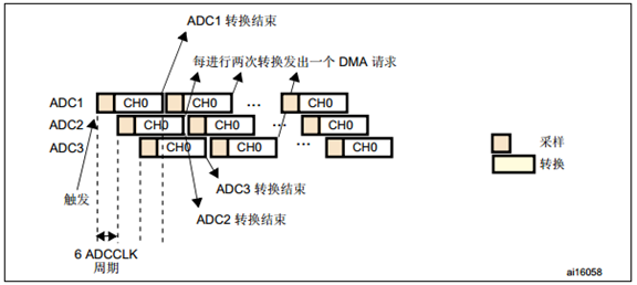
Figure 06 Triple ADC Crossover Mode
30.6.1 Hardware Design
The triple ADC cross mode is the ADC acquisition mode for the same channel. This situation is very similar to the single channel experiment of 00 subsections. It only uses three ADCs to collect the same channel at the same time, so the circuit design can be the same. Refer to Figure 05.
30.6.2 Software Design
Here only explain the core part of the code, some variable settings, header file inclusion, etc. are not involved, the complete code please refer to the supporting project in this chapter.
As with the single-channel routine, we write two ADC driver files, bsp_adc.h and bsp_adc.c, which are used to store the initialization functions of the IO pins used by the ADC and the ADC configuration-related functions. In fact, these two files are single-channel experiments. The files are very similar.
1. Programming points
1) Initialize the configuration ADC target pin to analog input mode;
2) Enable ADC1, ADC2, ADC3 and DMA clock;
3) Configure the DMA control to transfer the ADC general rule data register data to the specified storage area;
4) Configure the general-purpose ADC as the triple ADC alternate mode, sample 4 divide, use DMA mode 2;
5) Set ADC1, ADC2 and ADC3 to 12-bit resolution, disable scanning, continuous conversion, no external triggering required;
6) Set the conversion channel order and sampling time of ADC1, ADC2 and ADC3;
7) Enable DMA request of ADC1, and automatically request DMA for data transmission after ADC conversion;
8) Start ADC1, ADC2 and ADC3 conversion;
9) Enable software to trigger ADC conversion.
The ADC conversion result data is transferred to the specified memory area using DMA mode, which replaces the single channel experiment using the interrupt service read method.
2. Code analysis
ADC macro definition
Code Listing 011 Multichannel ADC Related Macro Definitions
1 #define RHEOSTAT_ADC_CDR_ADDR ((uint32_t)0x40012308)
2
3 #define RHEOSTAT_ADC_GPIO_PORT GPIOC
4 #define RHEOSTAT_ADC_GPIO_PIN GPIO_Pin_3
5 #define RHEOSTAT_ADC_GPIO_CLK RCC_AHB1Periph_GPIOC
6
7 #define RHEOSTAT_ADC1 ADC1
8 #define RHEOSTAT_ADC1_CLK RCC_APB2Periph_ADC1
9 #define RHEOSTAT_ADC2 ADC2
10 #define RHEOSTAT_ADC2_CLK RCC_APB2Periph_ADC2
11 #define RHEOSTAT_ADC3 ADC3
12 #define RHEOSTAT_ADC3_CLK RCC_APB2Periph_ADC3
13 #define RHEOSTAT_ADC_CHANNEL ADC_Channel_13
14
15 #define RHEOSTAT_ADC_DMA_CLK RCC_AHB1Periph_DMA2
16 #define RHEOSTAT_ADC_DMA_CHANNEL DMA_Channel_0
17 #define RHEOSTAT_ADC_DMA_STREAM DMA2_Stream0
Dual or triple ADCs require the general rule data register ADC_CDR, which is different from standalone mode. Define the potentiometer moving contact pin as the analog input to the triple ADC.
ADC GPIO initialization function
Code Listing 012 ADC GPIO Initialization
1 static void Rheostat_ADC_GPIO_Config(void)
2 {
3 GPIO_InitTypeDef GPIO_InitStructure;
4
5 // Enable GPIO clock
6 RCC_AHB1PeriphClockCmd(RHEOSTAT_ADC_GPIO_CLK, ENABLE);
7
8 // Configure IO
9 GPIO_InitStructure.GPIO_Pin = RHEOSTAT_ADC_GPIO_PIN;
10 // Configure as analog input
11 GPIO_InitStructure.GPIO_Mode = GPIO_Mode_AIN;
12 // Do not pull up or pull down
13 GPIO_InitStructure.GPIO_PuPd = GPIO_PuPd_NOPULL ;
14 GPIO_Init(RHEOSTAT_ADC_GPIO_PORT, &GPIO_InitStructure);
15 }
The corresponding GPIO clock must be enabled when using GPIO. The GPIO for AD conversion function must be configured as analog input mode.
Configure triple ADC alternate mode
Code Listing 013 Triple ADC Alternate Mode Configuration
1 static void Rheostat_ADC_Mode_Config(void)
2 {
3 DMA_InitTypeDef DMA_InitStructure;
4 ADC_InitTypeDef ADC_InitStructure;
5 ADC_CommonInitTypeDef ADC_CommonInitStructure;
6
7 // Turn on the ADC clock
8 RCC_APB2PeriphClockCmd(RHEOSTAT_ADC1_CLK , ENABLE);
9 RCC_APB2PeriphClockCmd(RHEOSTAT_ADC2_CLK , ENABLE);
10 RCC_APB2PeriphClockCmd(RHEOSTAT_ADC3_CLK , ENABLE);
11
12 // ------------------ DMA Init structure parameter initialization -----------------------
13 // ADC1 uses DMA2, data stream 0, channel 0, this is the manual fixed dead
14 // Turn on the DMA clock
15 RCC_AHB1PeriphClockCmd(RHEOSTAT_ADC_DMA_CLK, ENABLE);
16 // The peripheral base address is: ADC data register address
17 DMA_InitStructure.DMA_PeripheralBaseAddr = RHEOSTAT_ADC_CDR_ADDR;
18 // The memory address is actually an internal SRAM variable
19 DMA_InitStructure.DMA_Memory0BaseAddr = (u32)ADC_ConvertedValue;
20 // Data transfer direction is peripheral to memory
21 DMA_InitStructure.DMA_DIR = DMA_DIR_PeripheralToMemory;
22 // The buffer size is 3, the size of the buffer should be equal to the size of the memory
23 DMA_InitStructure.DMA_BufferSize = 3;
24 // There is only one peripheral register, the address does not increment
25 DMA_InitStructure.DMA_PeripheralInc = DMA_PeripheralInc_Disable;
26 // The memory address is automatically incremented
27 DMA_InitStructure.DMA_MemoryInc = DMA_MemoryInc_Enable;
28 // // Peripheral data size is word, ie four bytes
29 DMA_InitStructure.DMA_PeripheralDataSize=DMA_PeripheralDataSize_Word;
30 // The memory data size is also a word, the same size as the peripheral data
31 DMA_InitStructure.DMA_MemoryDataSize = DMA_MemoryDataSize_Word;
32 // Loop transfer mode
33 DMA_InitStructure.DMA_Mode = DMA_Mode_Circular;
34 // The DMA transfer channel priority is high. When using a DMA channel, the priority setting does not affect
35 DMA_InitStructure.DMA_Priority = DMA_Priority_High;
36 // Disable DMA FIFO, use direct connection mode
37 DMA_InitStructure.DMA_FIFOMode = DMA_FIFOMode_Disable;
38 // FIFO size, when FIFO mode is disabled, this is not configured
39 DMA_InitStructure.DMA_FIFOThreshold = DMA_FIFOThreshold_HalfFull;
40 DMA_InitStructure.DMA_MemoryBurst = DMA_MemoryBurst_Single;
41 DMA_InitStructure.DMA_PeripheralBurst = DMA_PeripheralBurst_Single;
42 // Select the DMA channel, the channel exists in the stream
43 DMA_InitStructure.DMA_Channel = RHEOSTAT_ADC_DMA_CHANNEL;
44 / / Initialize the DMA stream, the flow is equivalent to a large pipeline, there are many channels inside the pipeline
45 DMA_Init(RHEOSTAT_ADC_DMA_STREAM, &DMA_InitStructure);
46 // Enable DMA stream
47 DMA_Cmd(RHEOSTAT_ADC_DMA_STREAM, ENABLE);
48
49 // -------------------ADC Common Structure Parameter Initialization --------------------
50 // Triple ADC Alternating Mode
51 ADC_CommonInitStructure.ADC_Mode = ADC_TripleMode_Interl;
52 // The clock is divided by fpclk2 4
53 ADC_CommonInitStructure.ADC_Prescaler = ADC_Prescaler_Div4;
54 // Disable DMA direct access mode
55 ADC_CommonInitStructure.ADC_DMAAccessMode = ADC_DMAAccessMode_2;
56 // sampling interval
57 ADC_CommonInitStructure.ADC_TwoSamplingDelay =
58 ADC_TwoSamplingDelay_10Cycles;
59 ADC_CommonInit(&ADC_CommonInitStructure);
60
61 // ------------------- ADC Init Structure Parameter Initialization -----------------------
62 // ADC resolution
63 ADC_InitStructure.ADC_Resolution = ADC_Resolution_12b;
64 // Disable scanning mode, multi-channel acquisition is required
65 ADC_InitStructure.ADC_ScanConvMode = DISABLE;
66 // continuous conversion
67 ADC_InitStructure.ADC_ContinuousConvMode = ENABLE;
68 //Disable external edge trigger
69 ADC_InitStructure.ADC_ExternalTrigConvEdge =
70 ADC_ExternalTrigConvEdge_None;
71 //Use software trigger, external trigger does not need to be configured, comment out
72 //ADC_InitStructure.ADC_ExternalTrigConv=ADC_ExternalTrigConv_T1_CC1;
73 //Data right alignment
74 ADC_InitStructure.ADC_DataAlign = ADC_DataAlign_Right;
75 //Conversion channel 1
76 ADC_InitStructure.ADC_NbrOfConversion = 1;
77 ADC_Init(RHEOSTAT_ADC1, &ADC_InitStructure);
78 // Configure the ADC channel conversion sequence to 1, the first conversion, the sampling time is 3 clock cycles
79 ADC_RegularChannelConfig(RHEOSTAT_ADC1, RHEOSTAT_ADC_CHANNEL,
80 1, ADC_SampleTime_3Cycles);
81 //------------------------------------------------------------------
82 ADC_Init(RHEOSTAT_ADC2, &ADC_InitStructure);
83 // Configure the ADC channel conversion sequence to 1, the first conversion, the sampling time is 3 clock cycles
84 ADC_RegularChannelConfig(RHEOSTAT_ADC2, RHEOSTAT_ADC_CHANNEL,
85 1, ADC_SampleTime_3Cycles);
86 //------------------------------------------------------------------
87 ADC_Init(RHEOSTAT_ADC3, &ADC_InitStructure);
88 // Configure the ADC channel conversion sequence to 1, the first conversion, the sampling time is 3 clock cycles
89 ADC_RegularChannelConfig(RHEOSTAT_ADC3, RHEOSTAT_ADC_CHANNEL,
90 1, ADC_SampleTime_3Cycles);
91
92 // Enable DMA request after last transfer (multi-ADC mode)
93 ADC_MultiModeDMARequestAfterLastTransferCmd(ENABLE);
94 // Enable ADC DMA
95 ADC_DMACmd(RHEOSTAT_ADC1, ENABLE);
96 // Enable ADC
97 ADC_Cmd(RHEOSTAT_ADC1, ENABLE);
98 ADC_Cmd(RHEOSTAT_ADC2, ENABLE);
99 ADC_Cmd(RHEOSTAT_ADC3, ENABLE);
100
101 //Start adc conversion, software trigger
102 ADC_SoftwareStartConv(RHEOSTAT_ADC1);
103 ADC_SoftwareStartConv(RHEOSTAT_ADC2);
104 ADC_SoftwareStartConv(RHEOSTAT_ADC3);
105 }
First, we used DMA_InitTypeDef to define a DMA initialization type variable. We have already explained this in detail in DMA. In addition, we also use ADC_InitTypeDef and ADC_CommonInitTypeDef structure to define an ADC initialization and ADC common type variable respectively. The two structures have been explained in detail before.
Call RCC_APB2PeriphClockCmd() to turn on the ADC clock and RCC_AHB1PeriphClockCmd() to turn on the DMA clock.
We need to make the necessary configuration for the DMA. First set the peripheral base address is the ADC's general rule data register address; the memory address is the data storage area we specify, ADC_ConvertedValue is a global array name we define, it is an unsigned 32-bit integer number with three elements The ADC rule conversion corresponds to only one data register so the address cannot be incremented, and the storage area we specify also needs to increment the address. The ADC's general rule data register is valid for 32 bits. We configure the ADC to be DMA mode 2 and set the data size to the word size. The ADC is configured for continuous conversion mode and the DMA is also set to cyclic transmission mode. The DMA ADC channel is enabled after the DMA related parameters are set.
Next, we use ADC_CommonInitTypeDef structure variable ADC_CommonInitStructure to configure ADC as triple ADC alternate mode, division factor is 4, need to set DMA mode 2, 10 cycles of sampling delay, and call ADC_CommonInit function to complete ADC general working environment configuration.
We use ADC_InitTypeDef structure variable ADC_InitStructure to configure ADC1 to 12-bit resolution, no scan mode, start continuous conversion, use internal software trigger without external trigger event, use right-aligned data format, convert channel to 1, and call ADC_Init function to complete ADC1 working environment configuration. ADC2 and ADC3 can be configured in the same way as ADC1.
The ADC_RegularChannelConfig function is used to bind the ADC channel conversion order and sampling time. Bind the ADC channel pins and set the appropriate conversion order.
The ADC_MultiModeDMARequestAfterLastTransferCmd function controls whether the DMA request of the ADC is enabled. If the request is enabled and the ADC_DMACmd function is called to enable the DMA, the DMA is requested to implement data transfer after the ADC conversion is completed. Triple mode only needs to enable the DMA channel of ADC1.
The ADC_Cmd function controls the ADC conversion start and stop.
Finally, if you use a software trigger, you need to call the ADC_SoftwareStartConvCmd function to enable the configuration.
Main function
Code Listing 014 Main Function
1 int main(void)
2 {
3 / * Initialize USART1* /
4 Debug_USART_Config();
5
6 /*
7 Initialize the DAC used by the sliding rheostat. After the ADC data acquisition is completed, the data is directly transferred by the DMA.
8 ADC_ConvertedValue variable DMA directly changes the value of ADC_ConvertedValue*/
9 Rheostat_Init();
10
11 printf("\r\n ----This is an ADC experiment (DMA transfer)----\r\n");
12
13 while (1) {
14 Delay(0xffffee);
15 ADC_ConvertedValueLocal[0] =
16 (float)((uint16_t)ADC_ConvertedValue[0]*3.3/4096);
17 ADC_ConvertedValueLocal[1] =
18 (float)((uint16_t)ADC_ConvertedValue[2]*3.3/4096);
19 ADC_ConvertedValueLocal[2] =
20 (float)((uint16_t)ADC_ConvertedValue[1]*3.3/4096);
21 printf("\r\n The current AD value = 0x%08X \r\n",
22 ADC_ConvertedValue[0]);
23 printf("\r\n The current AD value = 0x%08X \r\n",
24 ADC_ConvertedValue[1]);
25 printf("\r\n The current AD value = 0x%08X \r\n",
26 ADC_ConvertedValue[2]);
27 printf("\r\n The current ADC1 value = %f V \r\n",
28 ADC_ConvertedValueLocal[0]);
29 printf("\r\n The current ADC2 value = %f V \r\n",
30 ADC_ConvertedValueLocal[1]);
31 printf("\r\n The current ADC3 value = %f V \r\n",
32 ADC_ConvertedValueLocal[2]);
33 }
34 }
The main function first calls the USARTx_Config function to configure the debugging serial port related parameters. The function is defined in the bsp_debug_usart.c file.
Next, call the Rheostat_Init function to initialize the ADC configuration and start the ADC. The Rheostat_Init function is defined in the bsp_adc.c file, which simply calls Rheostat_ADC_GPIO_Config() and Rheostat_ADC_Mode_Config() respectively.
The Delay function is just a simple delay function.
We configured the DMA data transfer so it will automatically save the data after the ADC conversion is completed to the array variable ADC_ConvertedValue. According to the data storage rule of DMA mode 2, the lower 16 bits of ADC_ConvertedValue[0] store ADC1 data and the upper 16 bits store ADC2 data. The lower 16 bits of ADC_ConvertedValue[1] store ADC3 data, the upper 16 bits store ADC1 data, the lower 16 bits of ADC_ConvertedValue[2] store ADC2 data, and the upper 16 bits store ADC3 data. We can extract the corresponding ADC conversion result as needed. data. The actual voltage corresponding to each ADC can be obtained by simple calculation.
The last is to print the relevant data to the serial debugging assistant.
30.6.3 Download verification
Ensure that the hardware connection of the development board is correct. Connect the USB TO UART interface to the computer with the USB cable, open the serial debugging assistant on the computer, and download the compiled program to the development board. In the serial port debugging assistant, you can see that there is continuous data transmission from the development board. At this time, we rotate the potentiometer to change its resistance value, then the corresponding data will also change.
30.7 One question per lesson
1. If the ADC resolution is set to 6, 8 or 10 bits, how is the input voltage value calculated?
2. According to the independent mode single channel acquisition experiment design to achieve the same function, it is required to use external hardware to trigger the conversion mode.
3. Write a dual ADC alternate mode program to implement an analog function similar to the triple ADC. It is required to use DMA mode 2 to implement the program function.
Intelligent Recommendation
STM32F4 DMA transfer measurements show that the ADC PWM
STM32F4 DMA transfer measurements show that the ADC PWM Talk is cheap ,show me your code !!! dma.c pwm.c adc.c Talk is cheap ,show me your code !!! main.c dma.c pwm.c adc.c...

STM32F4 series ADC converter quantity trap
STM32F4 series ADC converter quantity trap ADC quantity difference How to determine the number of ADCs of a certain type of MCU? Step 1: Enter STM32 official website -> Products -> STM32 Step 2:...
STM32F4 Peripheral Configuration Sample [ADC, DAC]
ADC principle ADC power requirements:full speedRun 2.4-3.6VSlowRunning 1.8V voltage input range V R E F − ≤ V I N ≤ V R E F + V_{REF-}\le V_{IN}\le V_{REF+} VREF−≤VIN≤VREF+ ...
[MCU learning] STM32F4 board ADC configuration
For personal reference only The ADC is transmitted by DMA, and there corresponds to each other, and the F4 board corresponds. To be supplemented...
STM32F4 ADC+DMA single channel collection
Background: Collect lithium battery voltage. Because the battery voltage is 12V, 12V has been divided into 12V in advance to ensure that the range of the ADC collection voltage is 0 ~ 3.3V. The collec...
More Recommendation
STM32F4 Series ADC - ADC Reuse Channel, Rule Channel and Injection Channel
STM32F4 Series ADC - ADC Reuse Channel, Rule Channel and Injection Channel ADC multiplexed channel External channel Internal channel Rule channel Inject passage Basic difference between rules channel ...
ADC use
One:ADC measuring battery voltage 1. As the battery voltage increases with the discharge time, the voltage will have a greater change, so it is necessary to monitor and display the battery voltage in ...
The use of ADC
Hardware basis The difference between ADC and ordinary IO port mode ADC interface on STM32F103 STM32F103 single -chip microcomputer has 2 module number converters one -one ADC (multi -channel multi -t...
STM32F4 multi-channel ADC 7 ADC (Double ADC Multi-channel) (DMA)
STM32F4 multi-channel ADC 7 ADC (Double ADC Multi-channel) (DMA) I said that I have to say it. There is no problem with the general settings. is this 7, If there is 6 or 8 (even) Because double ADC, i...
STM32F4 backup SRAM use
STM32F4 provides 4KB of backup SRAM, which can be used to store data that is not lost when the program is developed (requires RTC coin battery support), especially some real-time modified data that ca...