A design of comb filter in delta-sigma analog-to-digital converter
tags: MATLAB FPGA Section 3: Communication and Signal Processing Delta-sigma analog-to-digital converter Comb filter
The delta-sigma A/D converter is widely used due to its high precision and easy implementation with standard digital CMOS technology. The digital decimation filter is an important part of it, which is usually realized by a multi-stage structure. Since the comb filter is a linear phase FIR filter with a simple structure, it is usually used as the first stage of a digital filter. In this paper, a comb filter is designed. The filter is used in the first stage of the digital filter in the delta-sigma analog-to-digital converter. It is realized in a cascade structure. The power consumption and area of the small filter. The filter circuit is designed with Verilog HDL, debugged and functionally simulated through ModelSim, and then the simulation results are imported into MATLAB for spectrum analysis. The analysis result shows that the stopband attenuation reaches 100 dB, and the system meets the functional requirements. Finally, the synthesis tool Synplify Pro 7.3 is used to synthesize and optimize the code, and a comprehensive netlist is generated, which proves that the filter system can be synthesized.
With the rapid development of computer, communication, and multimedia technologies, the electronics industry has formed a pattern dominated by digital technology, especially the semiconductor industry. The increasing digitization and integration of semiconductor technology has promoted the development of "embedded" or "hidden" models in the promotion of microcontrollers (MCU), digital signal processors (DSP), and micromechanical electronic systems (MEMS) The development of digital conversion technology [1]. Under the influence of these factors, people have begun to use a chip to realize a complete system. With the reliable accuracy, perfect reproducibility, greater flexibility and other excellent characteristics of digital signal processing technology, it has realized the difference between analog technology and The interface between digital systems-analog to digital converter. Although the integration of analog and digital components has many benefits, the use of pure analog chips in key functions will improve performance, which will promote the analog-to-digital conversion technology towards high precision and high speed [2]; And the analog-to-digital converter (ADC) Performance often determines the performance of the system.
now,A/DConverterThe development trend mainly has the following characteristics[2]:The structure is constantly simplified; the conversion speed is increased; the resolution is increased as much as possible at high speed.
Adopt oversamplingΔ-∑The analog-to-digital conversion form can improve the resolution of the converter more effectively while increasing the speed, and its accuracy has reached24Above. In the over-sampling delta-sigma A/D converter, the decimation filter filters out the out-of-band noise of the shaped over-sampling signal and reduces the sampling frequency to the Nyquist frequency of the baseband signal, finally obtaining a high-precision For digital signals, a multi-stage structure is usually used to implement a decimation filter. Because of the simple structure of the comb filter and its frequency response characteristics, it is usually used in the first stage; the subsequent stages are FIR decimators.
Analog-to-digital converters can be divided into two categories: traditional multi-bit converters (also known as Nyquist analog-to-digital converters) and one-bit over-sampling converters (also known as delta-sigma analog-to-digital converters).
The resolution of the Nyquist ADC using traditional technology depends on the matching of the on-chip precision DAC; such as: successive approximation (SAR) type, integral type, parallel conversion, pipeline conversion andFolding difference conversionADC etc. [2] are all limited by this limitation, it is difficult to achieve ADC resolution higher than 16-bit; if you want to achieve 16-bit resolution, you need complex high-order analog anti-aliasing filters, timing and amplitude Sampling and holding circuits with extremely small errors are extremely difficult and costly. High-resolution Nyquist ADCs usually use the Nyquist rate (the sampling frequency is approximately 2 times the maximum frequency of the input signal) as the sampling frequency. The Nyquist sampler requires a complex analog low-pass filter (also called an anti-aliasing filter) to limit the maximum frequency of the signal entering the analog-to-digital converter and sample-and-hold circuit.
2.1 Traditional analog to digital converter
2.1.1 Successive approximation conversion
The successive approximation conversion method has a wide range of applications in today's analog-to-digital conversion field. It compares the analog signal that needs to be converted with a known different reference voltage multiple times, so that the converted digital quantity is sequentially approximated in value Enter the corresponding value of the analog quantity. The characteristics of the successive approximation conversion method are: the conversion speed is higher, which can reach 1 million times per second (MPSP); in the case of lower than 12-bit resolution, the circuit implementation is cheaper than other conversion methods; the conversion time is determined. However, this conversion method requires a digital-to-analog conversion circuit. Because a high-precision digital-to-analog conversion circuit requires a higher resistance or capacitance matching network, the accuracy is not very high.
2.1.2 Integral conversion
Integral analog-to-digital conversion technology has a wide range of applications in the field of low-speed, high-precision measurement, especially in the field of digital instruments. The integral analog-to-digital conversion technology has two conversion methods, single integral and double integral. The working principle of single integral analog-to-digital conversion is to first convert the converted electrical signal into a period of time, and then count the time interval, thereby indirectly An analog-to-digital conversion method for converting analog quantities into digital quantities. Its main defect is that the conversion accuracy is not high, which is mainly affected by the ramp voltage generator, the accuracy of the comparator, and the stability of the clock pulse.
In order to improve the conversion accuracy of the integral converter under the same conditions, a double integral conversion method can be used. The double integral converter partially offsets the error caused by the ramp generator by integrating the analog input signal twice. The conversion accuracy. The characteristics of the double integral conversion method are as follows: the accuracy is high and can reach22Bit; strong anti-interference ability, due to the role of the integral capacitor, can greatly suppress high-frequency noise. However, its conversion speed is too slow, and the conversion accuracy decreases with the increase of the conversion rate.100~300Times(SPS)The corresponding conversion accuracy is12Bit. So this conversion method is mainly used in low speed and high speedAccuracy of the conversion area.
2.1.3 Parallel conversion
Parallel conversion method Among all analog-to-digital conversions, the conversion speed is the fastest, and parallel conversion is a direct analog-to-digital conversion method. It greatly reduces the intermediate steps of the conversion process, and each digital code is obtained almost at the same time. Therefore, the parallel conversion is also called the flashing conversion method. The main feature of parallel conversion is that its conversion speed is extremely fast, up to 50MPSP, which is especially suitable for high-speed conversion fields. The disadvantage is that the resolution is not high, generally below 10 bits; when the accuracy is high, the power consumption is large. This is mainly affected by the circuit implementation, because an N-bit parallel converter requires 2N-1 comparators and voltage divider resistors, so the higher the accuracy, the more the number of comparators, the more difficult it is to manufacture.
2.1.4 Pipeline conversion
The pipeline conversion mode is an improvement of the parallel conversion mode. It not only has the characteristics of high-speed parallel conversion, but also overcomes the problem of manufacturing difficulties. Take the 8-bit two-stage pipeline type as an example. Its conversion process is first to perform the first-level high 4-bit parallel blinking conversion to obtain the high 4-bit signal; then, the input analog signal is combined with the first-level converted digital signal. The indicated analog quantity is subtracted, and the difference obtained is sent to the second-stage parallel flicker converter to obtain the low 4-bit signal. The characteristics of the pipeline conversion method are: high precision, up to 16 bitsRight; the conversion speed is faster,16This type ofADCSpeed up5MPSP, Faster than the successive comparison type; under the same resolution, the circuit scale and power consumption are greatly reduced. However, the pipeline conversion method sacrifices speed in exchange for high precision, and there is still the possibility of conversion errors. That is, the range of the remaining signal of the first stage does not meet the second stage parallel flashingADCWhen the range is required, linear distortion or missing codes will occur, and additional circuits are needed for adjustment.
2.1.5 Folding difference conversion
The fold-interpolation conversion method overcomes the speed drop caused by the pipelined step-by-step conversion. Through the preprocessing circuit, high and low data are obtained at the same time, but the number of components is greatly reduced. Folding interpolation conversion method signal preprocessing method is folding—that is, to map the larger input signal to a smaller area and convert it into a digital signal. This data is the low-order data of the entire digital quantity; Find out the interval where the input signal is mapped. This interval is also represented by a digital quantity. This data is the high-order data of the entire digital quantity. The high and low data are processed to get the final digital signal.
The characteristics of the folding interpolation conversion method are: the two quantizations of the data are carried out at the same time, with the characteristics of parallel conversion, and the speed; the circuit scale and power consumption are not large, such as8Bit converter only40A comparator. When the signal frequency is too high, the folding interpolation method requires additional processing circuits; and when the number of bits exceeds8If you want to keep the number of comparators small, folding interpolation becomes very troublesome, so it is generally only used for8WithIn the converter below.
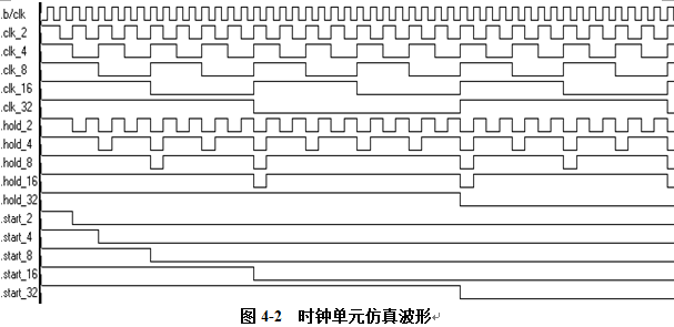
The design of the flip-flop belongs to the part of sequential logic design. The edge-sensitive memory cell of the flip-flop is synchronized by the rising or falling edge of a certain signal (usually called a clock signal). D flip-flop is one of the simplest flip-flops. It stores the current value of the D input terminal on the first valid edge of the clock. This value has nothing to do with the currently stored data; it can also be used as a clock delay. The block diagram of the 1-bit D flip-flop module and its truth table are shown in Figure 4-3 and Table 4-1, respectively.
The following is the written Verilog HDL code, which lists the 1-bit D flip-flop, 1-bit decimator, and 5-bit adder.
(1) Program list 4-1 Clock code
`timescale 1ns/1ps
module clk(clk,reset,clk_2,clk_4,clk_8,clk_16,clk_32, hold_2,hold_4,hold_8,
hold_16,hold_32, start_2,start_4,start_8,start_16,start_32);
input clk,reset;
output clk_2,clk_4,clk_8,clk_16,clk_32;
output start_2,start_4,start_8,start_16,start_32;
output hold_2,hold_4,hold_8,hold_16,hold_32;
reg hold_2,hold_4,hold_8,hold_16,hold_32;
reg[4:0] count;
reg start_2,start_4,start_8,start_16,start_32;
wire clk_32=~count[4],clk_16=~count[3],clk_8=~count[2],clk_4=~count[1], clk_2=~count[0];
always @(posedge clk or posedge reset)
if (reset)
begin
hold_2<=1; hold_4<=1; hold_8<=1; hold_16<=1; hold_32<=1;
count<=0;
start_2<=1; start_4<=1; start_8<=1; start_16<=1; start_32<=1;
end
else
begin
count<=count+1;
if(count==5'b11111)
begin
hold_2<=0; hold_4<=0; hold_8<=0; hold_16<=0; hold_32<=0; start_32<=0;
end
else if(count==15)
begin
hold_2<=0; hold_4<=0; hold_8<=0; hold_16<=0; start_16<=0;
end
else if(count==7)
begin
hold_2<=0; hold_4<=0; hold_8<=0; start_8<=0;
end
else if(count[1:0]==2'b11)
begin
hold_2<=0; hold_4<=0; start_4<=0;
end
else if(count[0]==1)
begin
hold_2<=0; start_2<=0;
end
else begin
hold_2<=1; hold_4<=1; hold_8<=1; hold_16<=1;
end
end
endmodule
(2) Program list 4-2 1-digit D trigger code
`timescale 1ns/1ps
module D_s(data_in,reset,clk,data_out);
parameter size=1;
input [size-1:0]data_in;
input reset;
input clk;
output[size-1:0] data_out=4'b0;
reg[size-1:0] data_out;
always @(posedge clk)
if(reset)
data_out<=0;
else
data_out<=data_in;
endmodule
(3) Program list 4-3 1-digit extractor code
`timescale 1ns/1ps
module samp1(data_out,data_in,hold,clk,reset);
parameter size=1;
output[size-1:0]data_out;
input[size-1:0]data_in;
input clk,hold,reset;
reg[size-1:0]data_out=1'b0;
always @(posedge clk)
if(reset)
data_out<=0;
else
if (hold)
data_out<=data_out;
else
data_out<=data_in;
endmodule
(4) Program list 4-4 5-digit adder code
`timescale 1ns/1ps
module sum5(in_a,in_b,cin,sum,c);
parameter size=5;
output c;
output [size-1:0]sum;
input [size-1:0]in_a,in_b;
input cin;
assign {c,sum}=in_a+in_b+cin;
endmodule
(5) Program list 4-5 Cascade structure level 1 code
`timescale 1ns/1ps
module stage0(out,in,start_2,clk,clk_2,hold_2,reset);
parameter size=1;
input in;
input clk,reset;
input hold_2;
input clk_2;
input start_2;
output[size+3:0] out;
wire clk_2,clk_4,clk_8,clk_16,clk_32, start_2,start_4,start_8,start_16,start_32;
wire hold_2,hold_4,hold_8,hold_16,hold_32;
wire [size-1:0] ploy_0,ploy_1,ploy_2;
wire [size+3:0] ploy00,ploy11,ploy22;
wire[size+3:0] sum1,sum2,sum3;
wire[size+3:0] out;
wire c1,c2,c3,c4;
wire c1_D,c2_D,c3_D,c4_D;
wire[size-1:0] data_D;
wire[size-1:0] x0_1,x0_2;
wire[size+3:0] x0_11,x0_22;
wire[size+3:0] y1,y0;
wire[size+3:0] x1_D,x2_D,x3_D;
assign out=y0+y1;
samp1 S1(ploy_0,in,hold_2,clk,reset);
D_s DD(in,reset,clk,data_D);
samp1 S2(ploy_1,data_D,hold_2,clk,reset);
D_s DD1(ploy_1,start_2,clk_2,ploy_2);
D_s DD2(ploy_0,start_2,clk_2,x0_1);
D_s DD3(x0_1,start_2,clk_2,x0_2);
assign x0_11={4'b0,x0_1},x0_22={4'b0,x0_2},ploy00={4'b0,ploy_0},
ploy11={4'b0,ploy_1}, ploy22={4'b0,ploy_2}; // Bit extension
// H0(z)
D_s D4(c1,start_2,clk_2,c1_D);
sum5 F1(ploy00,x0_22,c1_D,sum1,c1);
D_s D5(c2,start_2,clk_2,c2_D);
D_s_5 D6(x0_22,start_2,clk_2,x2_D);
sum5 F2(x2_D,x0_22,c2_D,sum2,c2);
D_s D7(c3,start_2,clk_2,c3_D);
sum5 F3(sum1,sum2,c3_D,y0,c3);
// H1(z)
D_s D8(c4,start_2,clk_2,c4_D);
sum5 F4(ploy11,ploy22,c4_D,sum3,c4);
D_s_5 D9(sum3,start_2,clk_2,x3_D);
D_s_5 D10(x3_D,start_2,clk_2,y1);
endmodule
(6) Program Listing 4-6 Comprehensive code of comb filter
`timescale 1ns/1ps
module cmb(in,reset,clk,clk_2,clk_4,clk_8,clk_16,clk_32, hold_2,hold_4,hold_8,
hold_16,hold_32,start_2,start_4,start_8,start_16,start_32,out);
input in;
input reset;
input clk,clk_2,clk_4,clk_8,clk_16,clk_32;
input hold_2,hold_4,hold_8,hold_16,hold_32;
input start_2,start_4,start_8,start_16,start_32;
output [20:0] out;
wire [4:0] out0;
wire [8:0] out1;
wire [12:0] out2;
wire [16:0] out3;
wire clk_2,clk_4,clk_8,clk_16,clk_32, hold_2,hold_4,hold_8,hold_16,hold_32;
wire start_2,start_4,start_8,start_16,start_32;
integer MFile;
stage0 v0(out0,in,start_2,clk,clk_2,hold_2,reset);
stage1 v1(out1,out0,start_4,clk_2,clk_4,hold_4,start_2);
stage2 v2(out2,out1,start_8,clk_4,clk_8,hold_8,start_4);
stage3 v3(out3,out2,start_16,clk_8,clk_16,hold_16,start_8);
stage4 v4(out,out3,start_32,clk_16,clk_32,hold_32,start_16);
initial
begin
MFile=$fopen("open_comb_20k.txt"); // Open the document
if(!MFile)
begin
$display(" Could not open");
$finish;
end
end
always @(posedge clk_32)
begin
$fdisplay (MFile,"%d",out); // Display output in decimal
$fclose(MFile);
end
always @(posedge clk_32)
$display ("comb_out=%b",out); // Display output in the command box in binary
endmodule
(7) Program list 4-7 Comprehensive test code
`timescale 1ns/1ps
`include "cmb.v"
module test_cmb( );
parameter length=65536*6;
reg in;
reg reset;
reg clk;
reg mem[length-1:0] ;
wire[20:0] out;
integer k;
initial begin
in=0;
reset=1;
clk=0;
# 30 reset=0;
end
always # 10 clk=~clk;
Initial $readmemb("input_65536_6_20k.dat",mem); // Read in the modulated signal
initial for (k=0;k<length-1;k=k+1)
@(posedge clk)
begin
in=mem[k];
end
clk CLK(clk,reset,clk_2,clk_4,clk_8,clk_16,clk_32, hold_2,hold_4,hold_8,
hold_16,hold_32,start_2,start_4,start_8,start_16,start_32);
cmb T(in,reset,clk,clk_2,clk_4,clk_8,clk_16,clk_32, hold_2,hold_4,hold_8,
hold_16,hold_32,start_2,start_4,start_8,start_16,start_32,out);
endmodule
Intelligent Recommendation
Design digital microcomposter and digital Hilbert converter with FIR filter
1. Digital microcompany The amplitude response of the ideal digital microcompany is In the processing of the separation domain, if the micro -splitter is long m (the third type of filter), it will be ...
FBCF feedback comb filter design
FBCF structure diagram The difference equation of the feedback comb filter is b0x(n)+y(n)b*z-M*(-aM)=y(n)=b0x(n)-aMy(n-M) The transfer function is H(z)=b01+aMz-M The feedback comb filter is a s...

6. Analog-to-digital converter ADC
6. Analog-to-digital converter ADC 6.1 ADC structure and register description 6.2 ADC design example 6.2.1 Use ADC1 regular channel to achieve analog-to-digital conversion of external analog signals 6...
STM32---------ADC (Analog/Digital Converter)
Article Directory Preface 1. ADC definition 2. Analog signal 3. Digital signal IV. The process of analog-to-digital conversion V. Characteristics 6. Hardware circuit 1. Schematic diagram 2. Pins used ...
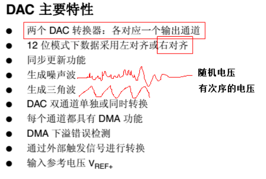
STM32----DAC (digital-to-analog converter)
Article Directory Preface 1. Overview 2. Main features 3. Hardware connection 1. Used PA4 and PA6 pins 2. Example of connection schematic diagram of PA4 and PA6 pins 4. Source code download Summarize ...
More Recommendation
Sigma-Delta ADC principle
Mainly I want to know how the Sigma-Delta ADC works, wrote a mess, piece of code to simply look. A very rough explanation, mainly give your own reference. SAR ADC The Successive Approximation Register...
sigma delta and LMS
1. sigma_delta There is a very classic thinking question in elementary school (brain teasers): find the thickness of a piece of paper in the textbook. Of course, the answer to this question is also ve...

Conversion of the analog filter to digital filter
In the blog post "Principle and realization of IIR Gaussian filter"We mentioned conversion from the s-domain to the z domain, that is, the analog filter into a digital filter Filter,This art...
Sigma sigma smoothing filter
Sigma sigma smoothing filter Reprinted from: https://www.cnblogs.com/Qsir/p/5802028.html Code. Effect picture...
Analysis of sigma delta modulator-the principle of sigma delta ADC
table of Contents The principle of Delta Sigma modulation is as follows Delta sigma modulation signal decoding delta sigma modulator for current sampling The principle of Delta Sigma modulation is as ...