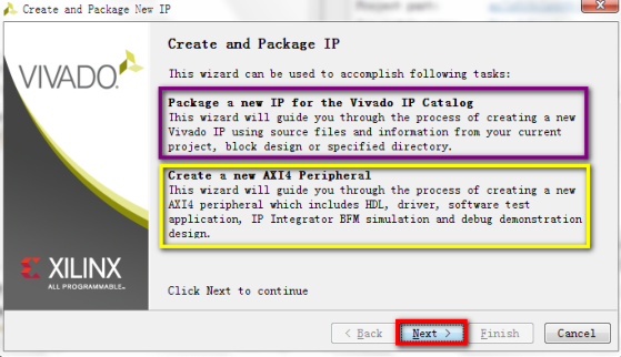
Creating AXI Master Interface IP and AXI4-Lite bus master reading and writing test from the timing Zynq-PL
tags: AXI_lite bus
Reprint: Original http://www.eefocus.com/antaur/blog/17-08/423751_6cc0d.html
0 Preface
By prior learning, you can create AXI interface IP core in slave mode PL side. But is the passive slave mode to receive data, but can not take the initiative to get the data, so plan to look at IP core construction method of AXI Master interface.
1. Using the wizard to create AXI Lite Master test case
In this step, the AXI type Lite type, optional parameters as follows:
Here, the focus is Interface Mode, previous experiments used the default configuration Slave, i.e. designed as a slave IP interface. In this experiment, to set it as Master.
The following three types of parameters with the parameters of the model can be configured Sl ** e is the same. Specific descriptions are as follows:
Data Width: bit-wide data bus is, in units of bits
Memory Size: Only IP type AXI FULLSlaveValid mode currently no discussions.
Number of Registers: Only IP interface type AXI LiteSlaveValid mode, described before can be found in the experiment.
At this point, create an AXI Lite Master type of IP interface has been configured using the Wizard tool.
2. Source analysis
2.1 top-level source code parsing
The system will automatically generate the IP of a project, you can view the generated source code and make modifications based on this.
As can be seen from the figure, the wizard tool generates two modules. Directly after synthesis, RTL-level view of the operation of FIG entry is as follows:
The results show the following:
Can be seen that only the top module made simple straight package, there is no internal logic design, see the code (Appendix 1) is true, the only useful operating parameters of the inner configuration module instance.
Measuring the specific configuration parameters are as follows:
You can see the configuration of the five parameters, including:
C_M00_AXI_ADDR_WIDTH indicates the address bus bit width, here configured to 32bits, as it relates to the bus protocol, it is recommended not to touch this parameter.
C_M00_AXI_DATA_WIDTH a data bus bit width, here configured to 32bits, for the same reason, it is recommended not to touch this parameter.
The remaining three parameters are related to the user logic test, the specific meaning will be explained in the analysis of the underlying source code module (Appendix 2), herein briefly explain:
C_M00_AXI_TARGET_SLAVE This represents BASE_ADDR IP hosts to be accessed as a slave memory base address.
C_M00_AXI_START_DATA_VALUE represents test data write operation to the slave registers
C_M00_AXI_TRANSACTIONS_NUM represent the number of tests
Significance specific logic and the parameters of the underlying parsing module See below.
2.2 parses the underlying source code
Example wizard automatically generates the underlying module AzIP_AXI_Master_Ex1_v1_0_M00_AXI, the module type is not a Master IO standard interface, but rather a logical test operation of the user. The Master Read and Write and read and write logic is not completed package, require careful analysis split sample code.
See the back of the specific code analysis described in Appendix 2 comments given here are merely notes I obtained this analysis.
- Test business logic
Nature of the business logic of the test shown below, is a typical testing process of memory read and write operations.
Code state machine manner using the preparation.
among them:
[Address] operational analysis:
From the initial address of the slave registers are variableC_M00_AXI_TARGET_SLAVE_BASE_ADDRDefined, when building integrated systems, from the corresponding memory mapped machine must be in the same configuration.
Write to the address bus as binding on the bus AXI,C_M00_AXI_TARGET_SLAVE_BASE_ADDRThe base address, the address offset axi_awaddr defined.
The address offset value of the initialization period0After each successful write address offset+4This is because the address defined in bytesByteAnd the data bus32bits, which is4Bytes, and therefore did not write32bitsWill be spent from the machine4Addresses of storage space.
Address definition and processing on a read operation is similar to the specified register.
[Analysis] data manipulation:
Write data bus used bound to an internal register.
During initialization, the test data register is set to the value of the configuration parameters, one after each addition.
After the test data from a writing machine, an internal backup saving, in the register expected_rdata code is as follows:
We can see exactly the same code logic, but the entire code architecture really beg to differ.
Comparing code data block is as follows:
Corresponding logic should be a mistake once, read_mismatch it is set to 1, if a next of the data status register remains 1 until the reset operation.
(2) AXI4-Lite bus interface definition
During AXI4-Lite bus read and write timing operation, we must first clear read and write interface bus.
View the technical documentation, this is mainly used in the following two technical documents:
- ARM's release of "ARM AMBA AXI Protocol v2.0 Specification"
- Xilinx has released the "Vivado Design Suite: AXI Reference Guide" UG1037 (v3.0) 2015
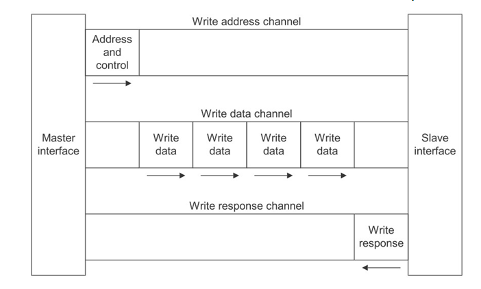
We can see that both AXI4 bus or a streamlined version of the AXI4-Lite bus interface is divided into five categories, which in turn are five categories **** in the operation of nuclear Read Write operation.
Write Operation
- Write Address: Master -> slave
- Write data: Master -> slave
- Write reply: Slave -> Host
Read Operation
- Read address: Master -> slave
- Read Data: Slave -> Host
The following focuses on what AXI4-Lite bus specifically how to define it and AXI4 bus protocol What is the difference?
First look at the official definition AXI4 bus protocol:
Look at the official definition of AXI4-Lite bus protocol:
It does not support the burst (Burst) transmission mode, and burst length = 1
32bit data bus width can only 64bits or the
Does not support exclusive access (exclusive accesses)
I.e. AXI4-Lite does not support the burst (Burst) transmission mode.
[Description] When the analysis focused behind the write timing on a burst (Burst) transmission mode is employed. Here the first foreshadowing it.
AXI4 bus, since the read-write channel is separate and can provide real-time bidirectional data transmission.
A burst (Burst) transmission mode, the transmission may be performed after an address, data burst to support up to 256words. (Words ?? 2 ?? bytes)
The following look at AXI4-Lite bus protocolPhysical InterfacePort definition:
5 can be seen that in addition to the type of signal channel clock and reset signals, is described in the foregoing.
But as a simplified bus protocol, physical interfaces should be better than the full version of AXI4 bus less, streamlined out specifically what? The table below.
After you learn the basics of principle, we look at examples of program code meets the official standards.
Analysis Example AXI Master Port IP source code definitions, i.e., codes of notes is as follows:
【AXI4-Lite Write Address Channel】
In the example program, M_AXI_AWPROT pin AXI Master module is always output as: 3'b000
【AXI4-Lite Write data Channel】
Which M_AXI_AWPROT port M_AXI_ARPROT, see [AXI4-Lite Write Address Channel] in
【AXI4-Lite Read Data Channel】
In the example program, AXI Master module because the data bus width is 32bit, so M_AXI_WSTRB pin is always output as: 4'b1111
【AXI4-Lite Write response Channel】
【AXI4-Lite Read Address Channel】
Which M_AXI_AWPROT port M_AXI_ARPROT, see [AXI4-Lite Write Address Channel] in
【AXI4-Lite Read Data Channel】
Where the port M_AXI_RRESP, see [AXI4-Lite Write response Channel] in M_AXI_BRESP
Where the port M_AXI_RRESP, see [AXI4-Lite Write response Channel] in M_AXI_BRESP
(3) AXI4-Lite bus read and write timing of the write operation timing analysis 1--
The timing of the interaction studies bus protocol, the protocol must rely on the standard, but can be found on the official protocol standards are not read and write timing AXI4-Lite bus independent timing settings.
Xilinx has released documents cited or ARM's published documentation, write timing diagram for the bus as follows:
Said host needs to write the address, and then write a series of data, why is the four temporary uncertainty from the machine after a response processed reply response.
ARM has released the document "ARM AMBA AXI Protocol v2.0 Specification" is not written AXI4-Lits of sequential logic, only timing diagram of the Write brust. As follows
After the previous studies, it is known AXI4-Lite brust length = Write brust 1, so I own simplified timing diagram of the above is as follows:
If the host continuously transmits two data write operation, I guess timing logic diagram should be as follows:
Analysis of the sample program, AXI Master source code module, to draw the corresponding host write data from the sequential logic unit as shown below:
View Code, the principle of timing analysis to get the timing and get personal analysis is not an exact match. Click here to bedding, we will hereinafter timing simulation and analysis of sample source, to obtain a corresponding sequence available for future use when writing their own interfaces. I remember watching below.
(4) AXI4-Lite bus read and write timing of the reading operation timing analysis 2--
Also learn about the first official agreement.
And a timing diagram of a read operation from official documents.
Also own analysis for brust length = AXI4-Lite bus 1, the read operation timing chart is shown below
Operation timing of the sample code not here in the drawing process flowchart. Hereinafter will be given exemplary timing relationships employed by timing simulation.
Timing analysis (5) Examples of projects
[Original starting point of the project created]:
According to the analysis of the AXI4-Lite bus interface, in fact, the data communication between the master and slave. AXI4-Lite Sl to create the association between the IP core ** e example, whether to create a top-level module directly connected AXI4-Lite Sl ** e exemplary IP core with AXI4-Lite Sl ** e IP core sample directly, complete AXI4-Lite bus read and write operations?
To verify the above idea, then create a first AXI4-Lite Sl ** e exemplary IP core parameters, and parameters to be exemplary AXI4-Lite Master core to a corresponding IP, the port is defined below the comparison as follows:
From the comparison chart, it can be seen from the interface AXI4-Lite master machine is in fact one matched.
Create a top-level file Top_AXI4_Lite_Interfce_Demo, generated from the sample directly connected to the master. Code in Appendix 3. The respective hierarchical structure as shown in FIG.
End Integrated RTL level connection as shown in FIG.
Create a simulation driving the top-level file, the code is as follows:
`timescale 1ns / 1ps
module Sim_AXI4_Lite_Interface();
reg axi_ACLK;// AXI bus clock
reg axi_ARESETn;// the system reset signal, active low
reg r_app_txn;// reset signal application level, a negative pulse, the rising edge of the reset
wire w_err;// status indication, abnormal
wire w_txn_done;// status indicator, has been sent
Top_AXI4_Lite_Interfce_Demo Ut1 (
.axi_ACLK(axi_ACLK),
.axi_ARESETn(axi_ARESETn),
.app_TXn(r_app_txn),
.state_err(w_err),
.state_done(w_txn_done)
);
parameter PERIOD = 2;
always begin
#(PERIOD/2);
axi_ACLK = ~axi_ACLK;
end
initial begin
axi_ACLK = 1'b0;
axi_ARESETn = 1'b1;
r_app_txn = 1'b1;
#(10*PERIOD);
axi_ARESETn = 1'b0;
#(5*PERIOD);
r_app_txn = 1'b0;
#(2*PERIOD);
axi_ARESETn = 1'b1;
#(4*PERIOD);
r_app_txn = 1'b1;
end
endmodule
After running the simulation results are as follows:
The simulation results of 1: 4 first written and then read 4 times the timing simulation results
Simulation results2: First written1Times, then read1Times timing simulation results
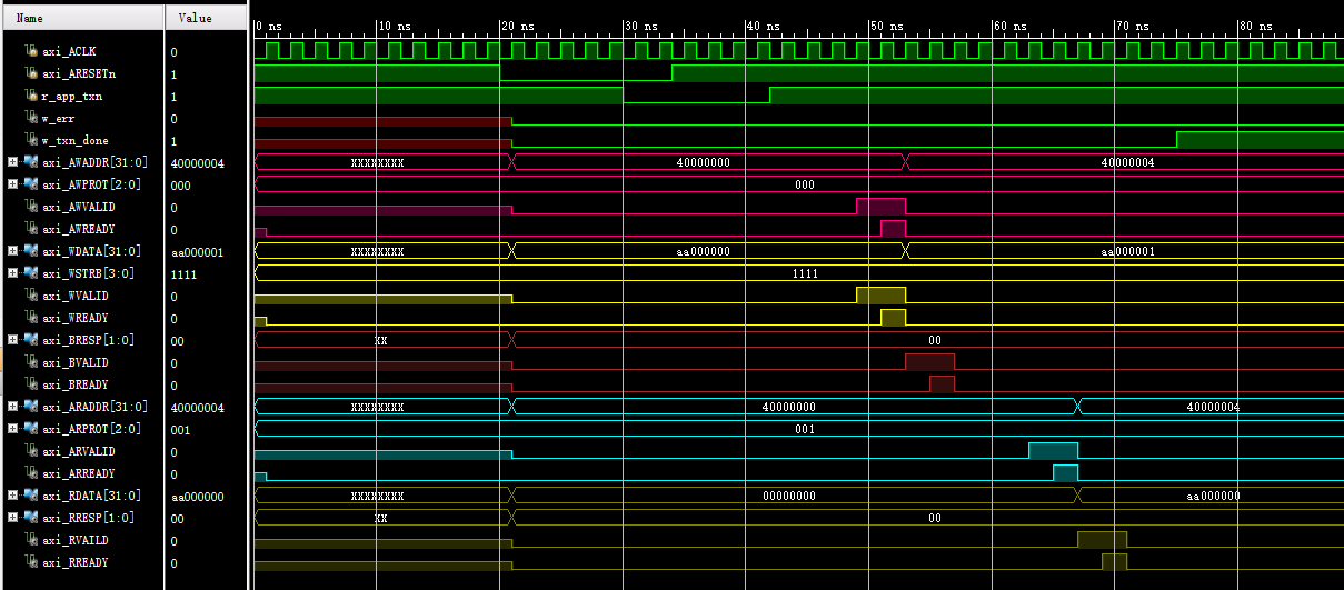
Simulation results3: Write only1Second timing simulation results
Simulation results 4: read only once timing simulation results
Simulation results5: First written2Times, then reading2Second timing simulation results
- Write timing contrast obtained by simulation and timing analysis document obtained from the official website
[Personal experience]
As can be seen, the AXI4 set type passage 5 are independent of each other, the simulation examples, and should AWVALID WVALID simultaneously to the slave, the slave on the bus and simultaneously sampling AWADDR WDATA data bus, and at the same time give the answer AWREADY and WREADY.
Slave Address and End after a match Data, an acknowledge BVALID.
The timing after starting address on the official document sent data, normal slave is able to respond correctly.
Conclusion, the preparation of their own interfaces, each channel to be processed independently, not coupled together.
- Read operation timing contrast obtained by simulation and timing analysis document obtained from the official website
[Personal experience]
Because without bus controller, but is directly connected, so timing simulation results from the response speed of the drawing machine quickly, and there is a response to the schematic processing delay.
2. summary
Through this study notes, a detailed analysis of the interaction process sequence AXI4-Lite bus master terminal, after master and slave can write their own interface to the machine.
Appendix 1: the top-level source code module:
`timescale 1ns / 1ps
module Top_AXI4_Lite_Interfce_Demo
#(
parameter C_AXI_START_DATA_VALUE = 32'hAA000000,
parameter C_AXI_TARGET_SLAVE_BASE_ADDR = 32'h40000000,
parameter integer C_AXI_ADDR_WIDTH = 32,
parameter integer C_AXI_DATA_WIDTH = 32,
parameter integer C_AXI_TRANSACTIONS_NUM = 4
)
(
input axi_ACLK,
input axi_ARESETn,
input app_TXn,
output state_err,
output state_done
);
wire w_err; // status indication, abnormal
wire w_txn_done; // status indication has been sent
assign state_err = w_err;
assign state_done = w_txn_done;
wire [C_AXI_ADDR_WIDTH-1: 0] axi_AWADDR; // AXI bus signals: AWADDR
wire [2: 0] axi_AWPROT; // AXI bus signals: AWPROT
wire axi_AWVALID; // AXI bus signals: AWVALID
wire axi_AWREADY; // AXI bus signals: AWREADY
wire [C_AXI_DATA_WIDTH-1: 0] axi_WDATA; // AXI bus signals: WDATA
wire [C_AXI_DATA_WIDTH / 8-1: 0] axi_WSTRB; // AXI bus signals: WSTRB
wire axi_WVALID; // AXI bus signals: WVALID
wire axi_WREADY; // AXI bus signals: WREADY
wire [1: 0] axi_BRESP; // AXI bus signals: BRESP
wire axi_BVALID; // AXI bus signals: BVALID
wire axi_BREADY; // AXI bus signals: BREADY
wire [C_AXI_ADDR_WIDTH-1: 0] axi_ARADDR; // AXI bus signals: ARADDR
wire [2: 0] axi_ARPROT; // AXI bus signals: ARPROT
wire axi_ARVALID; // AXI bus signals: ARVALID
wire axi_ARREADY; // AXI bus signals: ARREADY
wire [C_AXI_DATA_WIDTH-1: 0] axi_RDATA; // AXI bus signals: RDATA
wire [1: 0] axi_RRESP; // AXI bus signals: RRESP
wire axi_RVAILD; // AXI bus signals: RVAILD
wire axi_RREADY; // AXI bus signals: RREADY
axi_ip_master_v1_0 #
(
.C_M00_AXI_START_DATA_VALUE(C_AXI_START_DATA_VALUE),
.C_M00_AXI_TARGET_SLAVE_BASE_ADDR(C_AXI_TARGET_SLAVE_BASE_ADDR),
.C_M00_AXI_ADDR_WIDTH(C_AXI_ADDR_WIDTH),
.C_M00_AXI_DATA_WIDTH(C_AXI_DATA_WIDTH),
.C_M00_AXI_TRANSACTIONS_NUM(C_AXI_TRANSACTIONS_NUM)
) Ut1 (
//-- AXI4-Lite Global ----------------------------------------------
.m00_axi_aclk(axi_ACLK),
.m00_axi_aresetn(axi_ARESETn),
//------------------------------------------------------------------
.m00_axi_init_axi_txn(app_TXn),
.m00_axi_error(w_err),
.m00_axi_txn_done(w_txn_done),
//--- AXI4-Lite Write Address Channel ------------------------------
.m00_axi_awaddr(axi_AWADDR),
.m00_axi_awprot(axi_AWPROT),
.m00_axi_awvalid(axi_AWVALID),
.m00_axi_awready(axi_AWREADY),
//--- AXI4-Lite Write data Channel ------------------------------
.m00_axi_wdata(axi_WDATA),
.m00_axi_wstrb(axi_WSTRB),
.m00_axi_wvalid(axi_WVALID),
.m00_axi_wready(axi_WREADY),
//--- AXI4-Lite Write response Channel ------------------------------
.m00_axi_bresp(axi_BRESP),
.m00_axi_bvalid(axi_BVALID),
.m00_axi_bready(axi_BREADY),
//--- AXI4-Lite Read Address Channel ------------------------------
.m00_axi_araddr(axi_ARADDR),
.m00_axi_arprot(axi_ARPROT),
.m00_axi_arvalid(axi_ARVALID),
.m00_axi_arready(axi_ARREADY),
//--- AXI4-Lite Read Data Channel ------------------------------
.m00_axi_rdata(axi_RDATA),
.m00_axi_rresp(axi_RRESP),
.m00_axi_rvalid(axi_RVAILD),
.m00_axi_rready(axi_RREADY)
);
axi_ip_slave_v1_0 #
(
.C_S00_AXI_DATA_WIDTH(C_AXI_ADDR_WIDTH),
.C_S00_AXI_ADDR_WIDTH(7)
) Ut2 (
//-- AXI4-Lite Global ----------------------------------------------
.s00_axi_aclk(axi_ACLK),
.s00_axi_aresetn(axi_ARESETn),
//--- AXI4-Lite Write Address Channel ------------------------------
.s00_axi_awaddr (axi_AWADDR [6: 0]), // Note: Only the segment address! ! ! ! ! Do axi_slave_ip address bit width is 7, the number of registers 32
.s00_axi_awprot(axi_AWPROT),
.s00_axi_awvalid(axi_AWVALID),
.s00_axi_awready(axi_AWREADY),
//--- AXI4-Lite Write data Channel --------------------------------
.s00_axi_wdata(axi_WDATA),
.s00_axi_wstrb(axi_WSTRB),
.s00_axi_wvalid(axi_WVALID),
.s00_axi_wready(axi_WREADY),
//--- AXI4-Lite Write response Channel ------------------------------
.s00_axi_bresp(axi_BRESP),
.s00_axi_bvalid(axi_BVALID),
.s00_axi_bready(axi_BREADY),
//--- AXI4-Lite Read Address Channel ------------------------------
.s00_axi_araddr(axi_ARADDR),
.s00_axi_arprot(axi_ARPROT),
.s00_axi_arvalid(axi_ARVALID),
.s00_axi_arready(axi_ARREADY),
//--- AXI4-Lite Read Data Channel ------------------------------
.s00_axi_rdata(axi_RDATA),
.s00_axi_rresp(axi_RRESP),
.s00_axi_rvalid(axi_RVAILD),
.s00_axi_rready(axi_RREADY)
);
endmodule
Appendix 2: the underlying source code module MASTER top:
`timescale 1 ns / 1 ps
module axi_ip_master_v1_0 #
(
// Users to add parameters here
// User parameters ends
// Do not modify the parameters beyond this line
// Parameters of Axi Master Bus Interface M00_AXI
parameter C_M00_AXI_START_DATA_VALUE = 32'hAA000000,
parameter C_M00_AXI_TARGET_SLAVE_BASE_ADDR = 32'h40000000,
parameter integer C_M00_AXI_ADDR_WIDTH = 32,
parameter integer C_M00_AXI_DATA_WIDTH = 32,
parameter integer C_M00_AXI_TRANSACTIONS_NUM = 4
)
(
// Users to add ports here
// User ports ends
// Do not modify the ports beyond this line
// Ports of Axi Master Bus Interface M00_AXI
input wire m00_axi_init_axi_txn,
output wire m00_axi_error,
output wire m00_axi_txn_done,
input wire m00_axi_aclk,
input wire m00_axi_aresetn,
output wire [C_M00_AXI_ADDR_WIDTH-1 : 0] m00_axi_awaddr,
output wire [2 : 0] m00_axi_awprot,
output wire m00_axi_awvalid,
input wire m00_axi_awready,
output wire [C_M00_AXI_DATA_WIDTH-1 : 0] m00_axi_wdata,
output wire [C_M00_AXI_DATA_WIDTH/8-1 : 0] m00_axi_wstrb,
output wire m00_axi_wvalid,
input wire m00_axi_wready,
input wire [1 : 0] m00_axi_bresp,
input wire m00_axi_bvalid,
output wire m00_axi_bready,
output wire [C_M00_AXI_ADDR_WIDTH-1 : 0] m00_axi_araddr,
output wire [2 : 0] m00_axi_arprot,
output wire m00_axi_arvalid,
input wire m00_axi_arready,
input wire [C_M00_AXI_DATA_WIDTH-1 : 0] m00_axi_rdata,
input wire [1 : 0] m00_axi_rresp,
input wire m00_axi_rvalid,
output wire m00_axi_rready
);
// Instantiation of Axi Bus Interface M00_AXI
axi_ip_master_v1_0_M00_AXI # (
.C_M_START_DATA_VALUE(C_M00_AXI_START_DATA_VALUE),
.C_M_TARGET_SLAVE_BASE_ADDR(C_M00_AXI_TARGET_SLAVE_BASE_ADDR),
.C_M_AXI_ADDR_WIDTH(C_M00_AXI_ADDR_WIDTH),
.C_M_AXI_DATA_WIDTH(C_M00_AXI_DATA_WIDTH),
.C_M_TRANSACTIONS_NUM(C_M00_AXI_TRANSACTIONS_NUM)
) axi_ip_master_v1_0_M00_AXI_inst (
.INIT_AXI_TXN(m00_axi_init_axi_txn),
.ERROR(m00_axi_error),
.TXN_DONE(m00_axi_txn_done),
.M_AXI_ACLK(m00_axi_aclk),
.M_AXI_ARESETN(m00_axi_aresetn),
.M_AXI_AWADDR(m00_axi_awaddr),
.M_AXI_AWPROT(m00_axi_awprot),
.M_AXI_AWVALID(m00_axi_awvalid),
.M_AXI_AWREADY(m00_axi_awready),
.M_AXI_WDATA(m00_axi_wdata),
.M_AXI_WSTRB(m00_axi_wstrb),
.M_AXI_WVALID(m00_axi_wvalid),
.M_AXI_WREADY(m00_axi_wready),
.M_AXI_BRESP(m00_axi_bresp),
.M_AXI_BVALID(m00_axi_bvalid),
.M_AXI_BREADY(m00_axi_bready),
.M_AXI_ARADDR(m00_axi_araddr),
.M_AXI_ARPROT(m00_axi_arprot),
.M_AXI_ARVALID(m00_axi_arvalid),
.M_AXI_ARREADY(m00_axi_arready),
.M_AXI_RDATA(m00_axi_rdata),
.M_AXI_RRESP(m00_axi_rresp),
.M_AXI_RVALID(m00_axi_rvalid),
.M_AXI_RREADY(m00_axi_rready)
);
// Add user logic here
// User logic ends
endmodule
Appendix 3: bottom module MASTER underlying source:
`timescale 1 ns / 1 ps
module axi_ip_master_v1_0_M00_AXI #
(
// Users to add parameters here
// User parameters ends
// Do not modify the parameters beyond this line
// The master will start generating data from the C_M_START_DATA_VALUE value
parameter C_M_START_DATA_VALUE = 32'hAA000000,
// The master requires a target slave base address.
// The master will initiate read and write transactions on the slave with base address specified here as a parameter.
parameter C_M_TARGET_SLAVE_BASE_ADDR = 32'h40000000,
// Width of M_AXI address bus.
// The master generates the read and write addresses of width specified as C_M_AXI_ADDR_WIDTH.
parameter integer C_M_AXI_ADDR_WIDTH = 32,
// Width of M_AXI data bus.
// The master issues write data and accept read data where the width of the data bus is C_M_AXI_DATA_WIDTH
parameter integer C_M_AXI_DATA_WIDTH = 32,
// Transaction number is the number of write
// and read transactions the master will perform as a part of this example memory test.
parameter integer C_M_TRANSACTIONS_NUM = 4
)
(
// Users to add ports here
// User ports ends
// Do not modify the ports beyond this line
// Initiate AXI transactions
input wire INIT_AXI_TXN,
// Asserts when ERROR is detected
output reg ERROR,
// Asserts when AXI transactions is complete
output wire TXN_DONE,
// AXI clock signal
input wire M_AXI_ACLK,
// AXI active low reset signal
input wire M_AXI_ARESETN,
// Master Interface Write Address Channel ports. Write address (issued by master)
output wire [C_M_AXI_ADDR_WIDTH-1 : 0] M_AXI_AWADDR,
// Write channel Protection type.
// This signal indicates the privilege and security level of the transaction,
// and whether the transaction is a data access or an instruction access.
output wire [2 : 0] M_AXI_AWPROT,
// Write address valid.
// This signal indicates that the master signaling valid write address and control information.
output wire M_AXI_AWVALID,
// Write address ready.
// This signal indicates that the slave is ready to accept an address and associated control signals.
input wire M_AXI_AWREADY,
// Master Interface Write Data Channel ports. Write data (issued by master)
output wire [C_M_AXI_DATA_WIDTH-1 : 0] M_AXI_WDATA,
// Write strobes.
// This signal indicates which byte lanes hold valid data.
// There is one write strobe bit for each eight bits of the write data bus.
output wire [C_M_AXI_DATA_WIDTH/8-1 : 0] M_AXI_WSTRB,
// Write valid. This signal indicates that valid write data and strobes are available.
output wire M_AXI_WVALID,
// Write ready. This signal indicates that the slave can accept the write data.
input wire M_AXI_WREADY,
// Master Interface Write Response Channel ports.
// This signal indicates the status of the write transaction.
input wire [1 : 0] M_AXI_BRESP,
// Write response valid.
// This signal indicates that the channel is signaling a valid write response
input wire M_AXI_BVALID,
// Response ready. This signal indicates that the master can accept a write response.
output wire M_AXI_BREADY,
// Master Interface Read Address Channel ports. Read address (issued by master)
output wire [C_M_AXI_ADDR_WIDTH-1 : 0] M_AXI_ARADDR,
// Protection type.
// This signal indicates the privilege and security level of the transaction,
// and whether the transaction is a data access or an instruction access.
output wire [2 : 0] M_AXI_ARPROT,
// Read address valid.
// This signal indicates that the channel is signaling valid read address and control information.
output wire M_AXI_ARVALID,
// Read address ready.
// This signal indicates that the slave is ready to accept an address and associated control signals.
input wire M_AXI_ARREADY,
// Master Interface Read Data Channel ports. Read data (issued by slave)
input wire [C_M_AXI_DATA_WIDTH-1 : 0] M_AXI_RDATA,
// Read response. This signal indicates the status of the read transfer.
input wire [1 : 0] M_AXI_RRESP,
// Read valid. This signal indicates that the channel is signaling the required read data.
input wire M_AXI_RVALID,
// Read ready. This signal indicates that the master can accept the read data and response information.
output wire M_AXI_RREADY
);
// function called clogb2 that returns an integer which has the
// value of the ceiling of the log base 2
function integer clogb2 (input integer bit_depth);
begin
for(clogb2=0; bit_depth>0; clogb2=clogb2+1)
bit_depth = bit_depth >> 1;
end
endfunction
// TRANS_NUM_BITS is the width of the index counter for
// number of write or read transaction.
localparam integer TRANS_NUM_BITS = clogb2(C_M_TRANSACTIONS_NUM-1);
// Example State machine to initialize counter, initialize write transactions,
// initialize read transactions and comparison of read data with the
// written data words.
parameter [1:0] IDLE = 2'b00, // This state initiates AXI4Lite transaction
// after the state machine changes state to INIT_WRITE
// when there is 0 to 1 transition on INIT_AXI_TXN
INIT_WRITE = 2'b01, // This state initializes write transaction,
// once writes are done, the state machine
// changes state to INIT_READ
INIT_READ = 2'b10, // This state initializes read transaction
// once reads are done, the state machine
// changes state to INIT_COMPARE
INIT_COMPARE = 2'b11; // This state issues the status of comparison
// of the written data with the read data
reg [1:0] mst_exec_state;
// AXI4LITE signals
//write address valid
reg axi_awvalid;
//write data valid
reg axi_wvalid;
//read address valid
reg axi_arvalid;
//read data acceptance
reg axi_rready;
//write response acceptance
reg axi_bready;
//write address
reg [C_M_AXI_ADDR_WIDTH-1 : 0] axi_awaddr;
//write data
reg [C_M_AXI_DATA_WIDTH-1 : 0] axi_wdata;
//read addresss
reg [C_M_AXI_ADDR_WIDTH-1 : 0] axi_araddr;
//Asserts when there is a write response error
wire write_resp_error;
//Asserts when there is a read response error
wire read_resp_error;
//A pulse to initiate a write transaction
reg start_single_write;
//A pulse to initiate a read transaction
reg start_single_read;
//Asserts when a single beat write transaction is issued and remains asserted till the completion of write trasaction.
reg write_issued;
//Asserts when a single beat read transaction is issued and remains asserted till the completion of read trasaction.
reg read_issued;
//flag that marks the completion of write trasactions. The number of write transaction is user selected by the parameter C_M_TRANSACTIONS_NUM.
reg writes_done;
//flag that marks the completion of read trasactions. The number of read transaction is user selected by the parameter C_M_TRANSACTIONS_NUM
reg reads_done;
//The error register is asserted when any of the write response error, read response error or the data mismatch flags are asserted.
reg error_reg;
//index counter to track the number of write transaction issued
reg [TRANS_NUM_BITS : 0] write_index;
//index counter to track the number of read transaction issued
reg [TRANS_NUM_BITS : 0] read_index;
//Expected read data used to compare with the read data.
reg [C_M_AXI_DATA_WIDTH-1 : 0] expected_rdata;
//Flag marks the completion of comparison of the read data with the expected read data
reg compare_done;
//This flag is asserted when there is a mismatch of the read data with the expected read data.
reg read_mismatch;
//Flag is asserted when the write index reaches the last write transction number
reg last_write;
//Flag is asserted when the read index reaches the last read transction number
reg last_read;
reg init_txn_ff;
reg init_txn_ff2;
reg init_txn_edge;
wire init_txn_pulse;
// I/O Connections assignments
//Adding the offset address to the base addr of the slave
assign M_AXI_AWADDR = C_M_TARGET_SLAVE_BASE_ADDR + axi_awaddr;
//AXI 4 write data
assign M_AXI_WDATA = axi_wdata;
assign M_AXI_AWPROT = 3'b000;
assign M_AXI_AWVALID = axi_awvalid;
//Write Data(W)
assign M_AXI_WVALID = axi_wvalid;
//Set all byte strobes in this example
assign M_AXI_WSTRB = 4'b1111;
//Write Response (B)
assign M_AXI_BREADY = axi_bready;
//Read Address (AR)
assign M_AXI_ARADDR = C_M_TARGET_SLAVE_BASE_ADDR + axi_araddr;
assign M_AXI_ARVALID = axi_arvalid;
assign M_AXI_ARPROT = 3'b001;
//Read and Read Response (R)
assign M_AXI_RREADY = axi_rready;
//Example design I/O
assign TXN_DONE = compare_done;
assign init_txn_pulse = (!init_txn_ff2) && init_txn_ff;
//Generate a pulse to initiate AXI transaction.
always @(posedge M_AXI_ACLK)
begin
// Initiates AXI transaction delay
if (M_AXI_ARESETN == 0 )
begin
init_txn_ff <= 1'b0;
init_txn_ff2 <= 1'b0;
end
else
begin
init_txn_ff <= INIT_AXI_TXN;
init_txn_ff2 <= init_txn_ff;
end
end
//--------------------
//Write Address Channel
//--------------------
// The purpose of the write address channel is to request the address and
// command information for the entire transaction. It is a single beat
// of information.
// Note for this example the axi_awvalid/axi_wvalid are asserted at the same
// time, and then each is deasserted independent from each other.
// This is a lower-performance, but simplier control scheme.
// AXI VALID signals must be held active until accepted by the partner.
// A data transfer is accepted by the slave when a master has
// VALID data and the slave acknoledges it is also READY. While the master
// is allowed to generated multiple, back-to-back requests by not
// deasserting VALID, this design will add rest cycle for
// simplicity.
// Since only one outstanding transaction is issued by the user design,
// there will not be a collision between a new request and an accepted
// request on the same clock cycle.
always @(posedge M_AXI_ACLK)
begin
//Only VALID signals must be deasserted during reset per AXI spec
//Consider inverting then registering active-low reset for higher fmax
if (M_AXI_ARESETN == 0 || init_txn_pulse == 1'b1)
begin
axi_awvalid <= 1'b0;
end
//Signal a new address/data command is available by user logic
else
begin
if (start_single_write)
begin
axi_awvalid <= 1'b1;
end
//Address accepted by interconnect/slave (issue of M_AXI_AWREADY by slave)
else if (M_AXI_AWREADY && axi_awvalid)
begin
axi_awvalid <= 1'b0;
end
end
end
// start_single_write triggers a new write
// transaction. write_index is a counter to
// keep track with number of write transaction
// issued/initiated
always @(posedge M_AXI_ACLK)
begin
if (M_AXI_ARESETN == 0 || init_txn_pulse == 1'b1)
begin
write_index <= 0;
end
// Signals a new write address/ write data is
// available by user logic
else if (start_single_write)
begin
write_index <= write_index + 1;
end
end
//--------------------
//Write Data Channel
//--------------------
//The write data channel is for transfering the actual data.
//The data generation is speific to the example design, and
//so only the WVALID/WREADY handshake is shown here
always @(posedge M_AXI_ACLK)
begin
if (M_AXI_ARESETN == 0 || init_txn_pulse == 1'b1)
begin
axi_wvalid <= 1'b0;
end
//Signal a new address/data command is available by user logic
else if (start_single_write)
begin
axi_wvalid <= 1'b1;
end
//Data accepted by interconnect/slave (issue of M_AXI_WREADY by slave)
else if (M_AXI_WREADY && axi_wvalid)
begin
axi_wvalid <= 1'b0;
end
end
//----------------------------
//Write Response (B) Channel
//----------------------------
//The write response channel provides feedback that the write has committed
//to memory. BREADY will occur after both the data and the write address
//has arrived and been accepted by the slave, and can guarantee that no
//other accesses launched afterwards will be able to be reordered before it.
//The BRESP bit [1] is used indicate any errors from the interconnect or
//slave for the entire write burst. This example will capture the error.
//While not necessary per spec, it is advisable to reset READY signals in
//case of differing reset latencies between master/slave.
always @(posedge M_AXI_ACLK)
begin
if (M_AXI_ARESETN == 0 || init_txn_pulse == 1'b1)
begin
axi_bready <= 1'b0;
end
// accept/acknowledge bresp with axi_bready by the master
// when M_AXI_BVALID is asserted by slave
else if (M_AXI_BVALID && ~axi_bready)
begin
axi_bready <= 1'b1;
end
// deassert after one clock cycle
else if (axi_bready)
begin
axi_bready <= 1'b0;
end
// retain the previous value
else
axi_bready <= axi_bready;
end
//Flag write errors
assign write_resp_error = (axi_bready & M_AXI_BVALID & M_AXI_BRESP[1]);
//----------------------------
//Read Address Channel
//----------------------------
//start_single_read triggers a new read transaction. read_index is a counter to
//keep track with number of read transaction issued/initiated
always @(posedge M_AXI_ACLK)
begin
if (M_AXI_ARESETN == 0 || init_txn_pulse == 1'b1)
begin
read_index <= 0;
end
// Signals a new read address is
// available by user logic
else if (start_single_read)
begin
read_index <= read_index + 1;
end
end
// A new axi_arvalid is asserted when there is a valid read address
// available by the master. start_single_read triggers a new read
// transaction
always @(posedge M_AXI_ACLK)
begin
if (M_AXI_ARESETN == 0 || init_txn_pulse == 1'b1)
begin
axi_arvalid <= 1'b0;
end
//Signal a new read address command is available by user logic
else if (start_single_read)
begin
axi_arvalid <= 1'b1;
end
//RAddress accepted by interconnect/slave (issue of M_AXI_ARREADY by slave)
else if (M_AXI_ARREADY && axi_arvalid)
begin
axi_arvalid <= 1'b0;
end
// retain the previous value
end
//--------------------------------
//Read Data (and Response) Channel
//--------------------------------
//The Read Data channel returns the results of the read request
//The master will accept the read data by asserting axi_rready
//when there is a valid read data available.
//While not necessary per spec, it is advisable to reset READY signals in
//case of differing reset latencies between master/slave.
always @(posedge M_AXI_ACLK)
begin
if (M_AXI_ARESETN == 0 || init_txn_pulse == 1'b1)
begin
axi_rready <= 1'b0;
end
// accept/acknowledge rdata/rresp with axi_rready by the master
// when M_AXI_RVALID is asserted by slave
else if (M_AXI_RVALID && ~axi_rready)
begin
axi_rready <= 1'b1;
end
// deassert after one clock cycle
else if (axi_rready)
begin
axi_rready <= 1'b0;
end
// retain the previous value
end
//Flag write errors
assign read_resp_error = (axi_rready & M_AXI_RVALID & M_AXI_RRESP[1]);
//--------------------------------
//User Logic
//--------------------------------
//Address/Data Stimulus
//Address/data pairs for this example. The read and write values should
//match.
//Modify these as desired for different address patterns.
//Write Addresses
always @(posedge M_AXI_ACLK)
begin
if (M_AXI_ARESETN == 0 || init_txn_pulse == 1'b1)
begin
axi_awaddr <= 0;
end
// Signals a new write address/ write data is
// available by user logic
else if (M_AXI_AWREADY && axi_awvalid)
begin
axi_awaddr <= axi_awaddr + 32'h00000004;
end
end
// Write data generation
always @(posedge M_AXI_ACLK)
begin
if (M_AXI_ARESETN == 0 || init_txn_pulse == 1'b1 )
begin
axi_wdata <= C_M_START_DATA_VALUE;
end
// Signals a new write address/ write data is
// available by user logic
else if (M_AXI_WREADY && axi_wvalid)
begin
axi_wdata <= C_M_START_DATA_VALUE + write_index;
end
end
//Read Addresses
always @(posedge M_AXI_ACLK)
begin
if (M_AXI_ARESETN == 0 || init_txn_pulse == 1'b1)
begin
axi_araddr <= 0;
end
// Signals a new write address/ write data is
// available by user logic
else if (M_AXI_ARREADY && axi_arvalid)
begin
axi_araddr <= axi_araddr + 32'h00000004;
end
end
always @(posedge M_AXI_ACLK)
begin
if (M_AXI_ARESETN == 0 || init_txn_pulse == 1'b1)
begin
expected_rdata <= C_M_START_DATA_VALUE;
end
// Signals a new write address/ write data is
// available by user logic
else if (M_AXI_RVALID && axi_rready)
begin
expected_rdata <= C_M_START_DATA_VALUE + read_index;
end
end
//implement master command interface state machine
always @ ( posedge M_AXI_ACLK)
begin
if (M_AXI_ARESETN == 1'b0)
begin
// reset condition
// All the signals are assigned default values under reset condition
mst_exec_state <= IDLE;
start_single_write <= 1'b0;
write_issued <= 1'b0;
start_single_read <= 1'b0;
read_issued <= 1'b0;
compare_done <= 1'b0;
ERROR <= 1'b0;
end
else
begin
// state transition
case (mst_exec_state)
IDLE:
// This state is responsible to initiate
// AXI transaction when init_txn_pulse is asserted
if ( init_txn_pulse == 1'b1 )
begin
mst_exec_state <= INIT_WRITE;
ERROR <= 1'b0;
compare_done <= 1'b0;
end
else
begin
mst_exec_state <= IDLE;
end
INIT_WRITE:
// This state is responsible to issue start_single_write pulse to
// initiate a write transaction. Write transactions will be
// issued until last_write signal is asserted.
// write controller
if (writes_done)
begin
mst_exec_state <= INIT_READ;//
end
else
begin
mst_exec_state <= INIT_WRITE;
if (~axi_awvalid && ~axi_wvalid && ~M_AXI_BVALID && ~last_write && ~start_single_write && ~write_issued)
begin
start_single_write <= 1'b1;
write_issued <= 1'b1;
end
else if (axi_bready)
begin
write_issued <= 1'b0;
end
else
begin
start_single_write <= 1'b0; //Negate to generate a pulse
end
end
INIT_READ:
// This state is responsible to issue start_single_read pulse to
// initiate a read transaction. Read transactions will be
// issued until last_read signal is asserted.
// read controller
if (reads_done)
begin
mst_exec_state <= INIT_COMPARE;
end
else
begin
mst_exec_state <= INIT_READ;
if (~axi_arvalid && ~M_AXI_RVALID && ~last_read && ~start_single_read && ~read_issued)
begin
start_single_read <= 1'b1;
read_issued <= 1'b1;
end
else if (axi_rready)
begin
read_issued <= 1'b0;
end
else
begin
start_single_read <= 1'b0; //Negate to generate a pulse
end
end
INIT_COMPARE:
begin
// This state is responsible to issue the state of comparison
// of written data with the read data. If no error flags are set,
// compare_done signal will be asseted to indicate success.
ERROR <= error_reg;
mst_exec_state <= IDLE;
compare_done <= 1'b1;
end
default :
begin
mst_exec_state <= IDLE;
end
endcase
end
end //MASTER_EXECUTION_PROC
//Terminal write count
always @(posedge M_AXI_ACLK)
begin
if (M_AXI_ARESETN == 0 || init_txn_pulse == 1'b1)
last_write <= 1'b0;
//The last write should be associated with a write address ready response
else if ((write_index == C_M_TRANSACTIONS_NUM) && M_AXI_AWREADY)
last_write <= 1'b1;
else
last_write <= last_write;
end
//Check for last write completion.
//This logic is to qualify the last write count with the final write
//response. This demonstrates how to confirm that a write has been
//committed.
always @(posedge M_AXI_ACLK)
begin
if (M_AXI_ARESETN == 0 || init_txn_pulse == 1'b1)
writes_done <= 1'b0;
//The writes_done should be associated with a bready response
else if (last_write && M_AXI_BVALID && axi_bready)
writes_done <= 1'b1;
else
writes_done <= writes_done;
end
//------------------
//Read example
//------------------
//Terminal Read Count
always @(posedge M_AXI_ACLK)
begin
if (M_AXI_ARESETN == 0 || init_txn_pulse == 1'b1)
last_read <= 1'b0;
//The last read should be associated with a read address ready response
else if ((read_index == C_M_TRANSACTIONS_NUM) && (M_AXI_ARREADY) )
last_read <= 1'b1;
else
last_read <= last_read;
end
/*
Check for last read completion.
This logic is to qualify the last read count with the final read
response/data.
*/
always @(posedge M_AXI_ACLK)
begin
if (M_AXI_ARESETN == 0 || init_txn_pulse == 1'b1)
reads_done <= 1'b0;
//The reads_done should be associated with a read ready response
else if (last_read && M_AXI_RVALID && axi_rready)
reads_done <= 1'b1;
else
reads_done <= reads_done;
end
//-----------------------------
//Example design error register
//-----------------------------
//Data Comparison
always @(posedge M_AXI_ACLK)
begin
if (M_AXI_ARESETN == 0 || init_txn_pulse == 1'b1)
read_mismatch <= 1'b0;
//The read data when available (on axi_rready) is compared with the expected data
else if ((M_AXI_RVALID && axi_rready) && (M_AXI_RDATA != expected_rdata))
read_mismatch <= 1'b1;
else
read_mismatch <= read_mismatch;
end
// Register and hold any data mismatches, or read/write interface errors
always @(posedge M_AXI_ACLK)
begin
if (M_AXI_ARESETN == 0 || init_txn_pulse == 1'b1)
error_reg <= 1'b0;
//Capture any error types
else if (read_mismatch || write_resp_error || read_resp_error)
error_reg <= 1'b1;
else
error_reg <= error_reg;
end
// Add user logic here
// User logic ends
endmodule
Appendix 4: Slave top bottom module source code:
`timescale 1 ns / 1 ps
module axi_ip_slave_v1_0 #
(
// Users to add parameters here
// User parameters ends
// Do not modify the parameters beyond this line
// Parameters of Axi Slave Bus Interface S00_AXI
parameter integer C_S00_AXI_DATA_WIDTH = 32,
parameter integer C_S00_AXI_ADDR_WIDTH = 7
)
(
// Users to add ports here
// User ports ends
// Do not modify the ports beyond this line
// Ports of Axi Slave Bus Interface S00_AXI
input wire s00_axi_aclk,
input wire s00_axi_aresetn,
input wire [C_S00_AXI_ADDR_WIDTH-1 : 0] s00_axi_awaddr,
input wire [2 : 0] s00_axi_awprot,
input wire s00_axi_awvalid,
output wire s00_axi_awready,
input wire [C_S00_AXI_DATA_WIDTH-1 : 0] s00_axi_wdata,
input wire [(C_S00_AXI_DATA_WIDTH/8)-1 : 0] s00_axi_wstrb,
input wire s00_axi_wvalid,
output wire s00_axi_wready,
output wire [1 : 0] s00_axi_bresp,
output wire s00_axi_bvalid,
input wire s00_axi_bready,
input wire [C_S00_AXI_ADDR_WIDTH-1 : 0] s00_axi_araddr,
input wire [2 : 0] s00_axi_arprot,
input wire s00_axi_arvalid,
output wire s00_axi_arready,
output wire [C_S00_AXI_DATA_WIDTH-1 : 0] s00_axi_rdata,
output wire [1 : 0] s00_axi_rresp,
output wire s00_axi_rvalid,
input wire s00_axi_rready
);
// Instantiation of Axi Bus Interface S00_AXI
axi_ip_slave_v1_0_S00_AXI # (
.C_S_AXI_DATA_WIDTH(C_S00_AXI_DATA_WIDTH),
.C_S_AXI_ADDR_WIDTH(C_S00_AXI_ADDR_WIDTH)
) axi_ip_slave_v1_0_S00_AXI_inst (
.S_AXI_ACLK(s00_axi_aclk),
.S_AXI_ARESETN(s00_axi_aresetn),
.S_AXI_AWADDR(s00_axi_awaddr),
.S_AXI_AWPROT(s00_axi_awprot),
.S_AXI_AWVALID(s00_axi_awvalid),
.S_AXI_AWREADY(s00_axi_awready),
.S_AXI_WDATA(s00_axi_wdata),
.S_AXI_WSTRB(s00_axi_wstrb),
.S_AXI_WVALID(s00_axi_wvalid),
.S_AXI_WREADY(s00_axi_wready),
.S_AXI_BRESP(s00_axi_bresp),
.S_AXI_BVALID(s00_axi_bvalid),
.S_AXI_BREADY(s00_axi_bready),
.S_AXI_ARADDR(s00_axi_araddr),
.S_AXI_ARPROT(s00_axi_arprot),
.S_AXI_ARVALID(s00_axi_arvalid),
.S_AXI_ARREADY(s00_axi_arready),
.S_AXI_RDATA(s00_axi_rdata),
.S_AXI_RRESP(s00_axi_rresp),
.S_AXI_RVALID(s00_axi_rvalid),
.S_AXI_RREADY(s00_axi_rready)
);
// Add user logic here
// User logic ends
endmodule
Appendix 5: Slave underlying source code level modules:
//////// here need to explain: when do slave core, the number of registers is 32, after generating nuclear, address width of 7, and why? Because a 32-bit register is 4 bytes, so that a four registers occupy addresses. 2 ^ 7 = 128 addresses, a register is four.
`timescale 1 ns / 1 ps
module axi_ip_slave_v1_0_S00_AXI #
(
// Users to add parameters here
// User parameters ends
// Do not modify the parameters beyond this line
// Width of S_AXI data bus
parameter integer C_S_AXI_DATA_WIDTH = 32,
// Width of S_AXI address bus
parameter integer C_S_AXI_ADDR_WIDTH = 7
)
(
// Users to add ports here
// User ports ends
// Do not modify the ports beyond this line
// Global Clock Signal
input wire S_AXI_ACLK,
// Global Reset Signal. This Signal is Active LOW
input wire S_AXI_ARESETN,
// Write address (issued by master, acceped by Slave)
input wire [C_S_AXI_ADDR_WIDTH-1 : 0] S_AXI_AWADDR,
// Write channel Protection type. This signal indicates the
// privilege and security level of the transaction, and whether
// the transaction is a data access or an instruction access.
input wire [2 : 0] S_AXI_AWPROT,
// Write address valid. This signal indicates that the master signaling
// valid write address and control information.
input wire S_AXI_AWVALID,
// Write address ready. This signal indicates that the slave is ready
// to accept an address and associated control signals.
output wire S_AXI_AWREADY,
// Write data (issued by master, acceped by Slave)
input wire [C_S_AXI_DATA_WIDTH-1 : 0] S_AXI_WDATA,
// Write strobes. This signal indicates which byte lanes hold
// valid data. There is one write strobe bit for each eight
// bits of the write data bus.
input wire [(C_S_AXI_DATA_WIDTH/8)-1 : 0] S_AXI_WSTRB,
// Write valid. This signal indicates that valid write
// data and strobes are available.
input wire S_AXI_WVALID,
// Write ready. This signal indicates that the slave
// can accept the write data.
output wire S_AXI_WREADY,
// Write response. This signal indicates the status
// of the write transaction.
output wire [1 : 0] S_AXI_BRESP,
// Write response valid. This signal indicates that the channel
// is signaling a valid write response.
output wire S_AXI_BVALID,
// Response ready. This signal indicates that the master
// can accept a write response.
input wire S_AXI_BREADY,
// Read address (issued by master, acceped by Slave)
input wire [C_S_AXI_ADDR_WIDTH-1 : 0] S_AXI_ARADDR,
// Protection type. This signal indicates the privilege
// and security level of the transaction, and whether the
// transaction is a data access or an instruction access.
input wire [2 : 0] S_AXI_ARPROT,
// Read address valid. This signal indicates that the channel
// is signaling valid read address and control information.
input wire S_AXI_ARVALID,
// Read address ready. This signal indicates that the slave is
// ready to accept an address and associated control signals.
output wire S_AXI_ARREADY,
// Read data (issued by slave)
output wire [C_S_AXI_DATA_WIDTH-1 : 0] S_AXI_RDATA,
// Read response. This signal indicates the status of the
// read transfer.
output wire [1 : 0] S_AXI_RRESP,
// Read valid. This signal indicates that the channel is
// signaling the required read data.
output wire S_AXI_RVALID,
// Read ready. This signal indicates that the master can
// accept the read data and response information.
input wire S_AXI_RREADY
);
// AXI4LITE signals
reg [C_S_AXI_ADDR_WIDTH-1 : 0] axi_awaddr;
reg axi_awready;
reg axi_wready;
reg [1 : 0] axi_bresp;
reg axi_bvalid;
reg [C_S_AXI_ADDR_WIDTH-1 : 0] axi_araddr;
reg axi_arready;
reg [C_S_AXI_DATA_WIDTH-1 : 0] axi_rdata;
reg [1 : 0] axi_rresp;
reg axi_rvalid;
// Example-specific design signals
// local parameter for addressing 32 bit / 64 bit C_S_AXI_DATA_WIDTH
// ADDR_LSB is used for addressing 32/64 bit registers/memories
// ADDR_LSB = 2 for 32 bits (n downto 2)
// ADDR_LSB = 3 for 64 bits (n downto 3)
localparam integer ADDR_LSB = (C_S_AXI_DATA_WIDTH/32) + 1;
localparam integer OPT_MEM_ADDR_BITS = 4;
//----------------------------------------------
//-- Signals for user logic register space example
//------------------------------------------------
//-- Number of Slave Registers 32
reg [C_S_AXI_DATA_WIDTH-1:0] slv_reg0;
reg [C_S_AXI_DATA_WIDTH-1:0] slv_reg1;
reg [C_S_AXI_DATA_WIDTH-1:0] slv_reg2;
reg [C_S_AXI_DATA_WIDTH-1:0] slv_reg3;
reg [C_S_AXI_DATA_WIDTH-1:0] slv_reg4;
reg [C_S_AXI_DATA_WIDTH-1:0] slv_reg5;
reg [C_S_AXI_DATA_WIDTH-1:0] slv_reg6;
reg [C_S_AXI_DATA_WIDTH-1:0] slv_reg7;
reg [C_S_AXI_DATA_WIDTH-1:0] slv_reg8;
reg [C_S_AXI_DATA_WIDTH-1:0] slv_reg9;
reg [C_S_AXI_DATA_WIDTH-1:0] slv_reg10;
reg [C_S_AXI_DATA_WIDTH-1:0] slv_reg11;
reg [C_S_AXI_DATA_WIDTH-1:0] slv_reg12;
reg [C_S_AXI_DATA_WIDTH-1:0] slv_reg13;
reg [C_S_AXI_DATA_WIDTH-1:0] slv_reg14;
reg [C_S_AXI_DATA_WIDTH-1:0] slv_reg15;
reg [C_S_AXI_DATA_WIDTH-1:0] slv_reg16;
reg [C_S_AXI_DATA_WIDTH-1:0] slv_reg17;
reg [C_S_AXI_DATA_WIDTH-1:0] slv_reg18;
reg [C_S_AXI_DATA_WIDTH-1:0] slv_reg19;
reg [C_S_AXI_DATA_WIDTH-1:0] slv_reg20;
reg [C_S_AXI_DATA_WIDTH-1:0] slv_reg21;
reg [C_S_AXI_DATA_WIDTH-1:0] slv_reg22;
reg [C_S_AXI_DATA_WIDTH-1:0] slv_reg23;
reg [C_S_AXI_DATA_WIDTH-1:0] slv_reg24;
reg [C_S_AXI_DATA_WIDTH-1:0] slv_reg25;
reg [C_S_AXI_DATA_WIDTH-1:0] slv_reg26;
reg [C_S_AXI_DATA_WIDTH-1:0] slv_reg27;
reg [C_S_AXI_DATA_WIDTH-1:0] slv_reg28;
reg [C_S_AXI_DATA_WIDTH-1:0] slv_reg29;
reg [C_S_AXI_DATA_WIDTH-1:0] slv_reg30;
reg [C_S_AXI_DATA_WIDTH-1:0] slv_reg31;
wire slv_reg_rden;
wire slv_reg_wren;
reg [C_S_AXI_DATA_WIDTH-1:0] reg_data_out;
integer byte_index;
// I/O Connections assignments
assign S_AXI_AWREADY = axi_awready;
assign S_AXI_WREADY = axi_wready;
assign S_AXI_BRESP = axi_bresp;
assign S_AXI_BVALID = axi_bvalid;
assign S_AXI_ARREADY = axi_arready;
assign S_AXI_RDATA = axi_rdata;
assign S_AXI_RRESP = axi_rresp;
assign S_AXI_RVALID = axi_rvalid;
// Implement axi_awready generation
// axi_awready is asserted for one S_AXI_ACLK clock cycle when both
// S_AXI_AWVALID and S_AXI_WVALID are asserted. axi_awready is
// de-asserted when reset is low.
always @( posedge S_AXI_ACLK )
begin
if ( S_AXI_ARESETN == 1'b0 )
begin
axi_awready <= 1'b0;
end
else
begin
if (~axi_awready && S_AXI_AWVALID && S_AXI_WVALID)
begin
// slave is ready to accept write address when
// there is a valid write address and write data
// on the write address and data bus. This design
// expects no outstanding transactions.
axi_awready <= 1'b1;
end
else
begin
axi_awready <= 1'b0;
end
end
end
// Implement axi_awaddr latching
// This process is used to latch the address when both
// S_AXI_AWVALID and S_AXI_WVALID are valid.
always @( posedge S_AXI_ACLK )
begin
if ( S_AXI_ARESETN == 1'b0 )
begin
axi_awaddr <= 0;
end
else
begin
if (~axi_awready && S_AXI_AWVALID && S_AXI_WVALID)
begin
// Write Address latching
axi_awaddr <= S_AXI_AWADDR;
end
end
end
// Implement axi_wready generation
// axi_wready is asserted for one S_AXI_ACLK clock cycle when both
// S_AXI_AWVALID and S_AXI_WVALID are asserted. axi_wready is
// de-asserted when reset is low.
always @( posedge S_AXI_ACLK )
begin
if ( S_AXI_ARESETN == 1'b0 )
begin
axi_wready <= 1'b0;
end
else
begin
if (~axi_wready && S_AXI_WVALID && S_AXI_AWVALID)
begin
// slave is ready to accept write data when
// there is a valid write address and write data
// on the write address and data bus. This design
// expects no outstanding transactions.
axi_wready <= 1'b1;
end
else
begin
axi_wready <= 1'b0;
end
end
end
// Implement memory mapped register select and write logic generation
// The write data is accepted and written to memory mapped registers when
// axi_awready, S_AXI_WVALID, axi_wready and S_AXI_WVALID are asserted. Write strobes are used to
// select byte enables of slave registers while writing.
// These registers are cleared when reset (active low) is applied.
// Slave register write enable is asserted when valid address and data are available
// and the slave is ready to accept the write address and write data.
assign slv_reg_wren = axi_wready && S_AXI_WVALID && axi_awready && S_AXI_AWVALID;
always @( posedge S_AXI_ACLK )
begin
if ( S_AXI_ARESETN == 1'b0 )
begin
slv_reg0 <= 0;
slv_reg1 <= 0;
slv_reg2 <= 0;
slv_reg3 <= 0;
slv_reg4 <= 0;
slv_reg5 <= 0;
slv_reg6 <= 0;
slv_reg7 <= 0;
slv_reg8 <= 0;
slv_reg9 <= 0;
slv_reg10 <= 0;
slv_reg11 <= 0;
slv_reg12 <= 0;
slv_reg13 <= 0;
slv_reg14 <= 0;
slv_reg15 <= 0;
slv_reg16 <= 0;
slv_reg17 <= 0;
slv_reg18 <= 0;
slv_reg19 <= 0;
slv_reg20 <= 0;
slv_reg21 <= 0;
slv_reg22 <= 0;
slv_reg23 <= 0;
slv_reg24 <= 0;
slv_reg25 <= 0;
slv_reg26 <= 0;
slv_reg27 <= 0;
slv_reg28 <= 0;
slv_reg29 <= 0;
slv_reg30 <= 0;
slv_reg31 <= 0;
end
else begin
if (slv_reg_wren)
begin
case ( axi_awaddr[ADDR_LSB+OPT_MEM_ADDR_BITS:ADDR_LSB] )
5'h00:
for ( byte_index = 0; byte_index <= (C_S_AXI_DATA_WIDTH/8)-1; byte_index = byte_index+1 )
if ( S_AXI_WSTRB[byte_index] == 1 ) begin
// Respective byte enables are asserted as per write strobes
// Slave register 0
slv_reg0[(byte_index*8) +: 8] <= S_AXI_WDATA[(byte_index*8) +: 8];
end
5'h01:
for ( byte_index = 0; byte_index <= (C_S_AXI_DATA_WIDTH/8)-1; byte_index = byte_index+1 )
if ( S_AXI_WSTRB[byte_index] == 1 ) begin
// Respective byte enables are asserted as per write strobes
// Slave register 1
slv_reg1[(byte_index*8) +: 8] <= S_AXI_WDATA[(byte_index*8) +: 8];
end
5'h02:
for ( byte_index = 0; byte_index <= (C_S_AXI_DATA_WIDTH/8)-1; byte_index = byte_index+1 )
if ( S_AXI_WSTRB[byte_index] == 1 ) begin
// Respective byte enables are asserted as per write strobes
// Slave register 2
slv_reg2[(byte_index*8) +: 8] <= S_AXI_WDATA[(byte_index*8) +: 8];
end
5'h03:
for ( byte_index = 0; byte_index <= (C_S_AXI_DATA_WIDTH/8)-1; byte_index = byte_index+1 )
if ( S_AXI_WSTRB[byte_index] == 1 ) begin
// Respective byte enables are asserted as per write strobes
// Slave register 3
slv_reg3[(byte_index*8) +: 8] <= S_AXI_WDATA[(byte_index*8) +: 8];
end
5'h04:
for ( byte_index = 0; byte_index <= (C_S_AXI_DATA_WIDTH/8)-1; byte_index = byte_index+1 )
if ( S_AXI_WSTRB[byte_index] == 1 ) begin
// Respective byte enables are asserted as per write strobes
// Slave register 4
slv_reg4[(byte_index*8) +: 8] <= S_AXI_WDATA[(byte_index*8) +: 8];
end
5'h05:
for ( byte_index = 0; byte_index <= (C_S_AXI_DATA_WIDTH/8)-1; byte_index = byte_index+1 )
if ( S_AXI_WSTRB[byte_index] == 1 ) begin
// Respective byte enables are asserted as per write strobes
// Slave register 5
slv_reg5[(byte_index*8) +: 8] <= S_AXI_WDATA[(byte_index*8) +: 8];
end
5'h06:
for ( byte_index = 0; byte_index <= (C_S_AXI_DATA_WIDTH/8)-1; byte_index = byte_index+1 )
if ( S_AXI_WSTRB[byte_index] == 1 ) begin
// Respective byte enables are asserted as per write strobes
// Slave register 6
slv_reg6[(byte_index*8) +: 8] <= S_AXI_WDATA[(byte_index*8) +: 8];
end
5'h07:
for ( byte_index = 0; byte_index <= (C_S_AXI_DATA_WIDTH/8)-1; byte_index = byte_index+1 )
if ( S_AXI_WSTRB[byte_index] == 1 ) begin
// Respective byte enables are asserted as per write strobes
// Slave register 7
slv_reg7[(byte_index*8) +: 8] <= S_AXI_WDATA[(byte_index*8) +: 8];
end
5'h08:
for ( byte_index = 0; byte_index <= (C_S_AXI_DATA_WIDTH/8)-1; byte_index = byte_index+1 )
if ( S_AXI_WSTRB[byte_index] == 1 ) begin
// Respective byte enables are asserted as per write strobes
// Slave register 8
slv_reg8[(byte_index*8) +: 8] <= S_AXI_WDATA[(byte_index*8) +: 8];
end
5'h09:
for ( byte_index = 0; byte_index <= (C_S_AXI_DATA_WIDTH/8)-1; byte_index = byte_index+1 )
if ( S_AXI_WSTRB[byte_index] == 1 ) begin
// Respective byte enables are asserted as per write strobes
// Slave register 9
slv_reg9[(byte_index*8) +: 8] <= S_AXI_WDATA[(byte_index*8) +: 8];
end
5'h0A:
for ( byte_index = 0; byte_index <= (C_S_AXI_DATA_WIDTH/8)-1; byte_index = byte_index+1 )
if ( S_AXI_WSTRB[byte_index] == 1 ) begin
// Respective byte enables are asserted as per write strobes
// Slave register 10
slv_reg10[(byte_index*8) +: 8] <= S_AXI_WDATA[(byte_index*8) +: 8];
end
5'h0B:
for ( byte_index = 0; byte_index <= (C_S_AXI_DATA_WIDTH/8)-1; byte_index = byte_index+1 )
if ( S_AXI_WSTRB[byte_index] == 1 ) begin
// Respective byte enables are asserted as per write strobes
// Slave register 11
slv_reg11[(byte_index*8) +: 8] <= S_AXI_WDATA[(byte_index*8) +: 8];
end
5'h0C:
for ( byte_index = 0; byte_index <= (C_S_AXI_DATA_WIDTH/8)-1; byte_index = byte_index+1 )
if ( S_AXI_WSTRB[byte_index] == 1 ) begin
// Respective byte enables are asserted as per write strobes
// Slave register 12
slv_reg12[(byte_index*8) +: 8] <= S_AXI_WDATA[(byte_index*8) +: 8];
end
5'h0D:
for ( byte_index = 0; byte_index <= (C_S_AXI_DATA_WIDTH/8)-1; byte_index = byte_index+1 )
if ( S_AXI_WSTRB[byte_index] == 1 ) begin
// Respective byte enables are asserted as per write strobes
// Slave register 13
slv_reg13[(byte_index*8) +: 8] <= S_AXI_WDATA[(byte_index*8) +: 8];
end
5'h0E:
for ( byte_index = 0; byte_index <= (C_S_AXI_DATA_WIDTH/8)-1; byte_index = byte_index+1 )
if ( S_AXI_WSTRB[byte_index] == 1 ) begin
// Respective byte enables are asserted as per write strobes
// Slave register 14
slv_reg14[(byte_index*8) +: 8] <= S_AXI_WDATA[(byte_index*8) +: 8];
end
5'h0F:
for ( byte_index = 0; byte_index <= (C_S_AXI_DATA_WIDTH/8)-1; byte_index = byte_index+1 )
if ( S_AXI_WSTRB[byte_index] == 1 ) begin
// Respective byte enables are asserted as per write strobes
// Slave register 15
slv_reg15[(byte_index*8) +: 8] <= S_AXI_WDATA[(byte_index*8) +: 8];
end
5'h10:
for ( byte_index = 0; byte_index <= (C_S_AXI_DATA_WIDTH/8)-1; byte_index = byte_index+1 )
if ( S_AXI_WSTRB[byte_index] == 1 ) begin
// Respective byte enables are asserted as per write strobes
// Slave register 16
slv_reg16[(byte_index*8) +: 8] <= S_AXI_WDATA[(byte_index*8) +: 8];
end
5'h11:
for ( byte_index = 0; byte_index <= (C_S_AXI_DATA_WIDTH/8)-1; byte_index = byte_index+1 )
if ( S_AXI_WSTRB[byte_index] == 1 ) begin
// Respective byte enables are asserted as per write strobes
// Slave register 17
slv_reg17[(byte_index*8) +: 8] <= S_AXI_WDATA[(byte_index*8) +: 8];
end
5'h12:
for ( byte_index = 0; byte_index <= (C_S_AXI_DATA_WIDTH/8)-1; byte_index = byte_index+1 )
if ( S_AXI_WSTRB[byte_index] == 1 ) begin
// Respective byte enables are asserted as per write strobes
// Slave register 18
slv_reg18[(byte_index*8) +: 8] <= S_AXI_WDATA[(byte_index*8) +: 8];
end
5'h13:
for ( byte_index = 0; byte_index <= (C_S_AXI_DATA_WIDTH/8)-1; byte_index = byte_index+1 )
if ( S_AXI_WSTRB[byte_index] == 1 ) begin
// Respective byte enables are asserted as per write strobes
// Slave register 19
slv_reg19[(byte_index*8) +: 8] <= S_AXI_WDATA[(byte_index*8) +: 8];
end
5'h14:
for ( byte_index = 0; byte_index <= (C_S_AXI_DATA_WIDTH/8)-1; byte_index = byte_index+1 )
if ( S_AXI_WSTRB[byte_index] == 1 ) begin
// Respective byte enables are asserted as per write strobes
// Slave register 20
slv_reg20[(byte_index*8) +: 8] <= S_AXI_WDATA[(byte_index*8) +: 8];
end
5'h15:
for ( byte_index = 0; byte_index <= (C_S_AXI_DATA_WIDTH/8)-1; byte_index = byte_index+1 )
if ( S_AXI_WSTRB[byte_index] == 1 ) begin
// Respective byte enables are asserted as per write strobes
// Slave register 21
slv_reg21[(byte_index*8) +: 8] <= S_AXI_WDATA[(byte_index*8) +: 8];
end
5'h16:
for ( byte_index = 0; byte_index <= (C_S_AXI_DATA_WIDTH/8)-1; byte_index = byte_index+1 )
if ( S_AXI_WSTRB[byte_index] == 1 ) begin
// Respective byte enables are asserted as per write strobes
// Slave register 22
slv_reg22[(byte_index*8) +: 8] <= S_AXI_WDATA[(byte_index*8) +: 8];
end
5'h17:
for ( byte_index = 0; byte_index <= (C_S_AXI_DATA_WIDTH/8)-1; byte_index = byte_index+1 )
if ( S_AXI_WSTRB[byte_index] == 1 ) begin
// Respective byte enables are asserted as per write strobes
// Slave register 23
slv_reg23[(byte_index*8) +: 8] <= S_AXI_WDATA[(byte_index*8) +: 8];
end
5'h18:
for ( byte_index = 0; byte_index <= (C_S_AXI_DATA_WIDTH/8)-1; byte_index = byte_index+1 )
if ( S_AXI_WSTRB[byte_index] == 1 ) begin
// Respective byte enables are asserted as per write strobes
// Slave register 24
slv_reg24[(byte_index*8) +: 8] <= S_AXI_WDATA[(byte_index*8) +: 8];
end
5'h19:
for ( byte_index = 0; byte_index <= (C_S_AXI_DATA_WIDTH/8)-1; byte_index = byte_index+1 )
if ( S_AXI_WSTRB[byte_index] == 1 ) begin
// Respective byte enables are asserted as per write strobes
// Slave register 25
slv_reg25[(byte_index*8) +: 8] <= S_AXI_WDATA[(byte_index*8) +: 8];
end
5'h1A:
for ( byte_index = 0; byte_index <= (C_S_AXI_DATA_WIDTH/8)-1; byte_index = byte_index+1 )
if ( S_AXI_WSTRB[byte_index] == 1 ) begin
// Respective byte enables are asserted as per write strobes
// Slave register 26
slv_reg26[(byte_index*8) +: 8] <= S_AXI_WDATA[(byte_index*8) +: 8];
end
5'h1B:
for ( byte_index = 0; byte_index <= (C_S_AXI_DATA_WIDTH/8)-1; byte_index = byte_index+1 )
if ( S_AXI_WSTRB[byte_index] == 1 ) begin
// Respective byte enables are asserted as per write strobes
// Slave register 27
slv_reg27[(byte_index*8) +: 8] <= S_AXI_WDATA[(byte_index*8) +: 8];
end
5'h1C:
for ( byte_index = 0; byte_index <= (C_S_AXI_DATA_WIDTH/8)-1; byte_index = byte_index+1 )
if ( S_AXI_WSTRB[byte_index] == 1 ) begin
// Respective byte enables are asserted as per write strobes
// Slave register 28
slv_reg28[(byte_index*8) +: 8] <= S_AXI_WDATA[(byte_index*8) +: 8];
end
5'h1D:
for ( byte_index = 0; byte_index <= (C_S_AXI_DATA_WIDTH/8)-1; byte_index = byte_index+1 )
if ( S_AXI_WSTRB[byte_index] == 1 ) begin
// Respective byte enables are asserted as per write strobes
// Slave register 29
slv_reg29[(byte_index*8) +: 8] <= S_AXI_WDATA[(byte_index*8) +: 8];
end
5'h1E:
for ( byte_index = 0; byte_index <= (C_S_AXI_DATA_WIDTH/8)-1; byte_index = byte_index+1 )
if ( S_AXI_WSTRB[byte_index] == 1 ) begin
// Respective byte enables are asserted as per write strobes
// Slave register 30
slv_reg30[(byte_index*8) +: 8] <= S_AXI_WDATA[(byte_index*8) +: 8];
end
5'h1F:
for ( byte_index = 0; byte_index <= (C_S_AXI_DATA_WIDTH/8)-1; byte_index = byte_index+1 )
if ( S_AXI_WSTRB[byte_index] == 1 ) begin
// Respective byte enables are asserted as per write strobes
// Slave register 31
slv_reg31[(byte_index*8) +: 8] <= S_AXI_WDATA[(byte_index*8) +: 8];
end
default : begin
slv_reg0 <= slv_reg0;
slv_reg1 <= slv_reg1;
slv_reg2 <= slv_reg2;
slv_reg3 <= slv_reg3;
slv_reg4 <= slv_reg4;
slv_reg5 <= slv_reg5;
slv_reg6 <= slv_reg6;
slv_reg7 <= slv_reg7;
slv_reg8 <= slv_reg8;
slv_reg9 <= slv_reg9;
slv_reg10 <= slv_reg10;
slv_reg11 <= slv_reg11;
slv_reg12 <= slv_reg12;
slv_reg13 <= slv_reg13;
slv_reg14 <= slv_reg14;
slv_reg15 <= slv_reg15;
slv_reg16 <= slv_reg16;
slv_reg17 <= slv_reg17;
slv_reg18 <= slv_reg18;
slv_reg19 <= slv_reg19;
slv_reg20 <= slv_reg20;
slv_reg21 <= slv_reg21;
slv_reg22 <= slv_reg22;
slv_reg23 <= slv_reg23;
slv_reg24 <= slv_reg24;
slv_reg25 <= slv_reg25;
slv_reg26 <= slv_reg26;
slv_reg27 <= slv_reg27;
slv_reg28 <= slv_reg28;
slv_reg29 <= slv_reg29;
slv_reg30 <= slv_reg30;
slv_reg31 <= slv_reg31;
end
endcase
end
end
end
// Implement write response logic generation
// The write response and response valid signals are asserted by the slave
// when axi_wready, S_AXI_WVALID, axi_wready and S_AXI_WVALID are asserted.
// This marks the acceptance of address and indicates the status of
// write transaction.
always @( posedge S_AXI_ACLK )
begin
if ( S_AXI_ARESETN == 1'b0 )
begin
axi_bvalid <= 0;
axi_bresp <= 2'b0;
end
else
begin
if (axi_awready && S_AXI_AWVALID && ~axi_bvalid && axi_wready && S_AXI_WVALID)
begin
// indicates a valid write response is available
axi_bvalid <= 1'b1;
axi_bresp <= 2'b0; // 'OKAY' response
end // work error responses in future
else
begin
if (S_AXI_BREADY && axi_bvalid)
//check if bready is asserted while bvalid is high)
//(there is a possibility that bready is always asserted high)
begin
axi_bvalid <= 1'b0;
end
end
end
end
// Implement axi_arready generation
// axi_arready is asserted for one S_AXI_ACLK clock cycle when
// S_AXI_ARVALID is asserted. axi_awready is
// de-asserted when reset (active low) is asserted.
// The read address is also latched when S_AXI_ARVALID is
// asserted. axi_araddr is reset to zero on reset assertion.
always @( posedge S_AXI_ACLK )
begin
if ( S_AXI_ARESETN == 1'b0 )
begin
axi_arready <= 1'b0;
axi_araddr <= 32'b0;
end
else
begin
if (~axi_arready && S_AXI_ARVALID)
begin
// indicates that the slave has acceped the valid read address
axi_arready <= 1'b1;
// Read address latching
axi_araddr <= S_AXI_ARADDR;
end
else
begin
axi_arready <= 1'b0;
end
end
end
// Implement axi_arvalid generation
// axi_rvalid is asserted for one S_AXI_ACLK clock cycle when both
// S_AXI_ARVALID and axi_arready are asserted. The slave registers
// data are available on the axi_rdata bus at this instance. The
// assertion of axi_rvalid marks the validity of read data on the
// bus and axi_rresp indicates the status of read transaction.axi_rvalid
// is deasserted on reset (active low). axi_rresp and axi_rdata are
// cleared to zero on reset (active low).
always @( posedge S_AXI_ACLK )
begin
if ( S_AXI_ARESETN == 1'b0 )
begin
axi_rvalid <= 0;
axi_rresp <= 0;
end
else
begin
if (axi_arready && S_AXI_ARVALID && ~axi_rvalid)
begin
// Valid read data is available at the read data bus
axi_rvalid <= 1'b1;
axi_rresp <= 2'b0; // 'OKAY' response
end
else if (axi_rvalid && S_AXI_RREADY)
begin
// Read data is accepted by the master
axi_rvalid <= 1'b0;
end
end
end
// Implement memory mapped register select and read logic generation
// Slave register read enable is asserted when valid address is available
// and the slave is ready to accept the read address.
assign slv_reg_rden = axi_arready & S_AXI_ARVALID & ~axi_rvalid;
always @(*)
begin
// Address decoding for reading registers
case ( axi_araddr[ADDR_LSB+OPT_MEM_ADDR_BITS:ADDR_LSB] )
5'h00 : reg_data_out <= slv_reg0;
5'h01 : reg_data_out <= slv_reg1;
5'h02 : reg_data_out <= slv_reg2;
5'h03 : reg_data_out <= slv_reg3;
5'h04 : reg_data_out <= slv_reg4;
5'h05 : reg_data_out <= slv_reg5;
5'h06 : reg_data_out <= slv_reg6;
5'h07 : reg_data_out <= slv_reg7;
5'h08 : reg_data_out <= slv_reg8;
5'h09 : reg_data_out <= slv_reg9;
5'h0A : reg_data_out <= slv_reg10;
5'h0B : reg_data_out <= slv_reg11;
5'h0C : reg_data_out <= slv_reg12;
5'h0D : reg_data_out <= slv_reg13;
5'h0E : reg_data_out <= slv_reg14;
5'h0F : reg_data_out <= slv_reg15;
5'h10 : reg_data_out <= slv_reg16;
5'h11 : reg_data_out <= slv_reg17;
5'h12 : reg_data_out <= slv_reg18;
5'h13 : reg_data_out <= slv_reg19;
5'h14 : reg_data_out <= slv_reg20;
5'h15 : reg_data_out <= slv_reg21;
5'h16 : reg_data_out <= slv_reg22;
5'h17 : reg_data_out <= slv_reg23;
5'h18 : reg_data_out <= slv_reg24;
5'h19 : reg_data_out <= slv_reg25;
5'h1A : reg_data_out <= slv_reg26;
5'h1B : reg_data_out <= slv_reg27;
5'h1C : reg_data_out <= slv_reg28;
5'h1D : reg_data_out <= slv_reg29;
5'h1E : reg_data_out <= slv_reg30;
5'h1F : reg_data_out <= slv_reg31;
default : reg_data_out <= 0;
endcase
end
// Output register or memory read data
always @( posedge S_AXI_ACLK )
begin
if ( S_AXI_ARESETN == 1'b0 )
begin
axi_rdata <= 0;
end
else
begin
// When there is a valid read address (S_AXI_ARVALID) with
// acceptance of read address by the slave (axi_arready),
// output the read dada
if (slv_reg_rden)
begin
axi_rdata <= reg_data_out; // register read data
end
end
end
// Add user logic here
// User logic ends
endmodule
Intelligent Recommendation

Take you to quickly get started with AXI4 bus-AXI4-FULL chapter (3) ---- Xilinx Axi4-FULL interface IP source simulation analysis (Master interface)
In front After connecting the SLAVE interface, this article continues to pack an IP of the AXI4-FULL-MASTER interface, learn the source code, and then simulate the waveform. 1. Call ip First create a ...

ZYNQ+Vivado2015.2 series (seven) software and hardware combined with Debug to observe the timing of each signal when reading and writing the AXI bus
In the previous section, we learned to create IP based on the AXI bus, but we still don't know the timing of each signal in the AXI protocol. This experiment is to observe the AXI bus signal through t...
AXI Basics Part 4-Using AXI VIP as a Protocol Check Tool for AXI4 Master Interface
This technical article comes from the "Xilinx Product Design and Function Debugging Skills" section of Xilinx Chinese Forum. For more information, please visit https://forums.xilinx.com/cn T...
ZynQ Development Series 6: Creating AXI IP Implementation PS Configuration of PL PL (Step 1)
Start interface selection in VivadoManage IP, Newly built a folder called Custom_ip specializes in IP core Create a new IP,Tools OpenCreate and Package New IP InIP Catalog You can see a lot of officia...
ZYNQ AXI4 (AXI-full) bus learning (two) establishing simulation
1. Brief description Use vivado to customize the package axi-full master IP, and also package a slave IP to facilitate the simulation of the signal. 2. Package IP 1) Open vivado and perform the follow...
More Recommendation

ZT step by step learning ZedBoard & Zynq (4): Based on AXI Lite bus-based slave device IP design
This section adds to an existing ARM PS system by using the Custom IP Wizard (ipwiz) in XPS.User-defined IP(Custom IP), understand the basic structure of AXI Lite IP, and masterAXI Lite IPThe customiz...
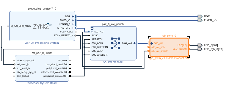
PYNQ PL generates pwm ip core, axi-lite bus + PS realizes breathing lights
Create the axi-lite bus yourself, to led rgbled output interface Need 4+3*2=10 regs as output Specific IP core internal add pwm.v Instantiate, reg because pwm has a fine granularity of 256, reg only u...

Take you to quickly get started with AXI4 bus-AXI4-LITE chapter (2) ---- Xilinx Axi4-Lite interface IP source simulation analysis (SLAVE interface)
In front In the Axis chapter, we packed the IP of 2 AXI4-Stream interface (one master and one, follower) (one master and one)Take you to quickly get started with AXI4 bus-AXI4-Stream chapter (2) ---- ...
Detailed explanation of AXI bus timing in ZYNQ
The AXI bus is a high-performance, high-bandwidth, and low-latency on-chip bus. The AXI protocol describes the method of data transmission between master and slave devices. The master device and the s...
Zynq Axi4 bus transfer IIC interface package
First, here IIC read and write the Verilog program that packs it, it is packaged as AXI4 IP, so it can be directly connected to the Zynq system. PL_IIC_ORIGINAL.V, IIC.V is a new file that is currentl...