Detailed explanation of SPI bus protocol and SPI timing diagram
tags: Embedded some knowledge SPI timing
SPI is the abbreviation of English Serial Peripheral Interface. As the name implies, it is a serial peripheral interface. SPI is a high-speed, full-duplex, synchronous communication bus, and it only occupies four wires on the pins of the chip, which saves the pins of the chip, and at the same time saves space and provides convenience for the PCB layout. Because of this simple and easy-to-use feature, more and more chips now integrate this communication protocol.
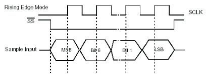
SPI is a ring bus structure, composed of ss(cs), sck, sdi, and sdo. The timing is actually very simple. The main reason is that two bidirectional shift registers exchange data under the control of sck.Rising edge sending, falling edge receiving, high bit first sending.
When the rising edge arrives, the level on sdo will be sent to the register of the slave device.
When the falling edge arrives, the level on sdi will be received into the register of the master device.
The SPI bus is a three-wire synchronous interface launched by Motorola. It communicates in a synchronous serial three-wire mode: a clock line SCK, a data input line MOSI, and a data output line MISO; it is used for full-duplex, full-duplex, and a Synchronous serial communication.
The main features of SPI are: it can send and receive serial data at the same time; can work as a master or a slave; provide a frequency programmable clock; send end interrupt flag; write conflict protection; bus competition protection, etc.
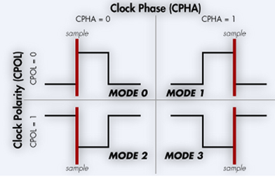
SPI bus has four working modes (SP0, SP1, SP2, SP3), of which the most widely used isSPI0 and SPI3 modes.
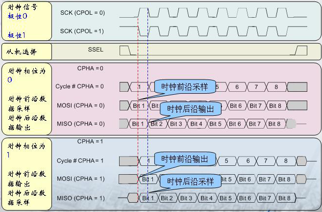
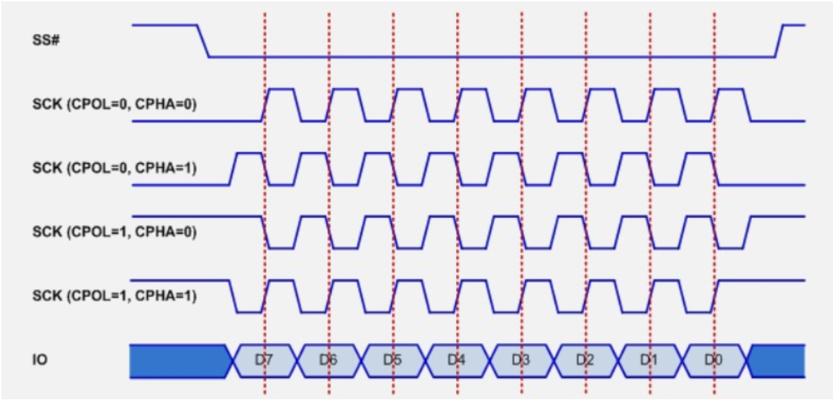
In order to exchange data with peripherals, the SPI module can configure the polarity and phase of its output serial synchronization clock according to the work requirements of the peripherals. The clock polarity (CPOL) has no significant impact on the transmission protocol. If CPOL=0, the idle state of the serial synchronous clock is low; if CPOL=1, the idle state of the serial synchronous clock is high. The clock phase (CPHA) can be configured to select one of two different transmission protocols for data transmission. If CPHA=0, the data is sampled on the first edge (rising or falling) of the serial synchronous clock; if CPHA=1, the data is sampled on the second edge (rising or falling) of the serial synchronous clock sampling. The phase and polarity of the SPI master module and the peripheral tone clock that communicate with it should be consistent.
Detailed SPI timing diagram-the moment when the SPI interface outputs the first data in mode 0
The moment when the SPI interface outputs the first bit of data in mode 0.
SPI interface has four different data transmission timings, depending on the combination of CPOL and CPHL. These four timings are shown in Figure 1.
The relationship between timing and CPOL and CPHL can also be seen from the figure.

CPOL is used to determine the level of the SCK clock signal when it is idle, CPOL=0, the idle level is low, and when CPOL=1, the idle level is high. CPHA is used to determine the sampling time, CPHA=0, sampling at the first clock edge of each cycle, CPHA=1, sampling at the second clock edge of each cycle. Since the device I used works in the timing of mode 0 (CPOL=0, CPHA=0), I simplified Figure 1 to Figure 2 and only focused on the timing of mode 0.
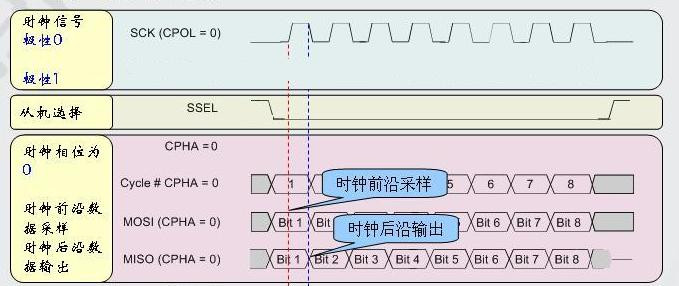
Let's focus on the first clock cycle of SCK, sampling data on the leading edge of the clock (rising edge, first clock edge), and outputting data on the back edge of the clock (falling edge, second clock edge). First look at the master device. The data bit1 output from the output port (MOSI) of the master device is sampled by the slave device at the leading edge of the clock. When does the master device output bit1? The output time of bit1 is actually half a clock cycle earlier than the rising edge of SCK before the SCK signal becomes valid. The output moment of bit1 has nothing to do with the SSEL signal. Looking at the slave device again, the input port MISO of the master device also samples the bit1 output by the slave device at the leading edge of the clock, so when does the slave device output bit1.The slave device outputs bit1 immediately after the SSEL signal is valid, although the SCK signal has not yet taken effect.The above master device and slave device output bit1 bit time can be verified from Figures 3 and 4.
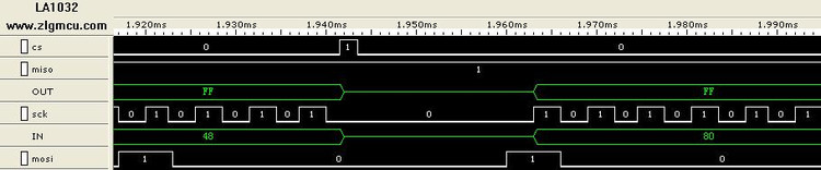
Note that in Figure 3, after the CS signal is valid (low level is valid, pay attention to what happens after the falling edge of CS), the delay program is used to delay for a period of time, and then the data to be sent is written to the data register. Observe the status (MOSI) of the output bit1 of the master device. It can be seen that bit1 (value 1) is output at half a clock cycle before the SCK signal is valid (it has nothing to do with the CS signal), and the rising edge of the first clock cycle of SCK is just sampled by the slave device.
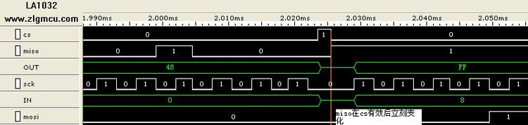
In Figure 4, pay attention to the CS and MISO signals. We can see that after the CS signal is valid, the slave device immediately outputs bit1 (the value is 1).
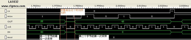
Usually the spi operations we perform are 16 bits. Figure 5 records the process of interconnection between the first byte and the second byte. The last bit of the first byte is sampled on the rising edge of SCK, and on the subsequent falling edge of SCK, the slave device outputs the first bit of the second byte.
Introduction to SPI bus protocol (interface definition, transmission timing)
1. Technical performance
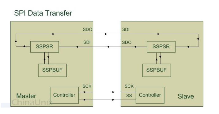
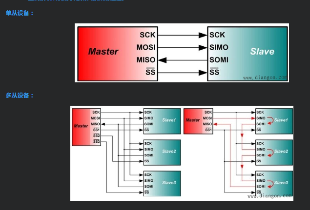
The SPI interface is a full-duplex three-wire synchronous serial peripheral interface first proposed by Motorola. It adopts a master-slave mode (Master-Slave) architecture; supports multi-slave mode applications and generally only supports a single master.
The clock is controlled by the Master. Under the clock shift pulse, the data is transmitted bit by bit, with the high bit in front and the low bit in the back (MSB first); the SPI interface has 2 unidirectional data lines, which are full-duplex communication. The data in the current application The speed can reach the level of several Mbps.
-------------------------------------------------------
Two, interface definition
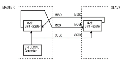
There are 4 signal lines in the SPI interface, namely: device selection line, clock line, serial output data line, and serial input data line.

(1) MOSI: Master device data output, slave device data input
(2) MISO: master device data input, slave device data output
(3) SCLK: clock signal, generated by the master device
(4) /SS: slave device enable signal, controlled by the master device
-------------------------------------------------------
Three, internal structure
Fourth, transmission timing
The internal hardware of the SPI interface is actually two simple shift registers. The transmitted data is 8 bits. Under the slave enable signal and shift pulse generated by the master device, it is transmitted bit by bit, with the high bit in front and the low bit in the back. . As shown in the figure below, the data changes on the falling edge of SCLK, and one bit of data on the rising edge is stored in the shift register.
SPI interface does not have designated flow control, and there is no response mechanism to confirm whether data is received.
Intelligent Recommendation
SPI bus protocol and driver
2019 Unicorn Enterprise Heavy Gold Recruitment Python Engineer Standard >>> Agreement introduction SPI (Serial Peripheral Interface), a serial peripheral interface, is a serial ...
spi bus protocol record
To excerpt: Overview: SPI, Serial Perripheral Interface, a serial peripheral interface is a synchronous serial interface technology proposed by Motorola. SPI peripherals physically connected to the mi...

On the SPI bus protocol
Introduction The SPI bus is a three-wire synchronous interface introduced by Motorola. It communicates in synchronous serial three-wire mode: one clock lineSCK, A data output lineMOSI(Master Output Sl...
SPI bus protocol
SPI (Serial Peripheral Interface), serial peripheral device interface, is a high-speed, full-duplex, and synchronous communication bus that occupies four wires on the pins of the chip. SPI is a ring b...

SPI bus protocol analysis
1. Brief introduction of SPI SPI is the abbreviation of English Serial Peripheral interface, as the name implies, is the serial peripheral interface. Motorola first defined it on its MC68HCXX series p...
More Recommendation

Communication protocol-SPI bus
One,SPIBus basic overview SPI, Is a high-speed, full-duplex, synchronous communication bus, and only occupies four lines on the chip pins,They are: 1)、MOSI——Mas...
STM32 SPI bus protocol
The SPI bus protocol is a serial peripheral device interface, a three-wire synchronous serial interface technology launched by Motorola Company, SPI is a high-speed, full-duplex, synchronous communica...
Bus Communication Protocol -SPI
table of Contents 1 Introduction 1.1 bus characteristics 1.2 Bus Interface: 1.3 working mode 2. Transport protocol 2.1 timing chart 2.2 Structure Diagram 2.3 Status Map: 2.4 code implementation 3. Sma...
SPI bus protocol overview
I. Overview SPI (Serial Peripheral Interface is a kindSynchronous serialCommunication protocol, byOne master device and one or more from devicesComposition, the master device starts with the switching...
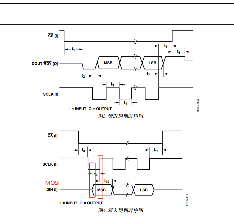
A sense of timing operations about the SPI bus protocol of the AD7193
Recently, I used the 24bit ADC chip in the project. In the process of the most driving operation, it took a lot of time, mainly to understand the timing of the bus, and the foundation is not prison. I...