Altium Designer Getting Started Notes (3) Wire Harness
tags: FPGA development
1. Wire Harness
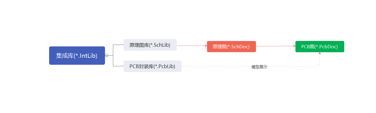
The wire harness carries multiple signals and may contain buses and wires. These harnesses are grouped and collectively referred to as single entities. This multi-signal connection is called "Signal Harness".
With “Signal Harness,” or the harness connector, a higher level of abstraction can be created and operated, and more complex designs can be presented with simpler layers.
1.1 Wire Harness Connector
A wiring harness connector is a type of terminal. A connector, also known as a plug, consists of a plug and a socket.
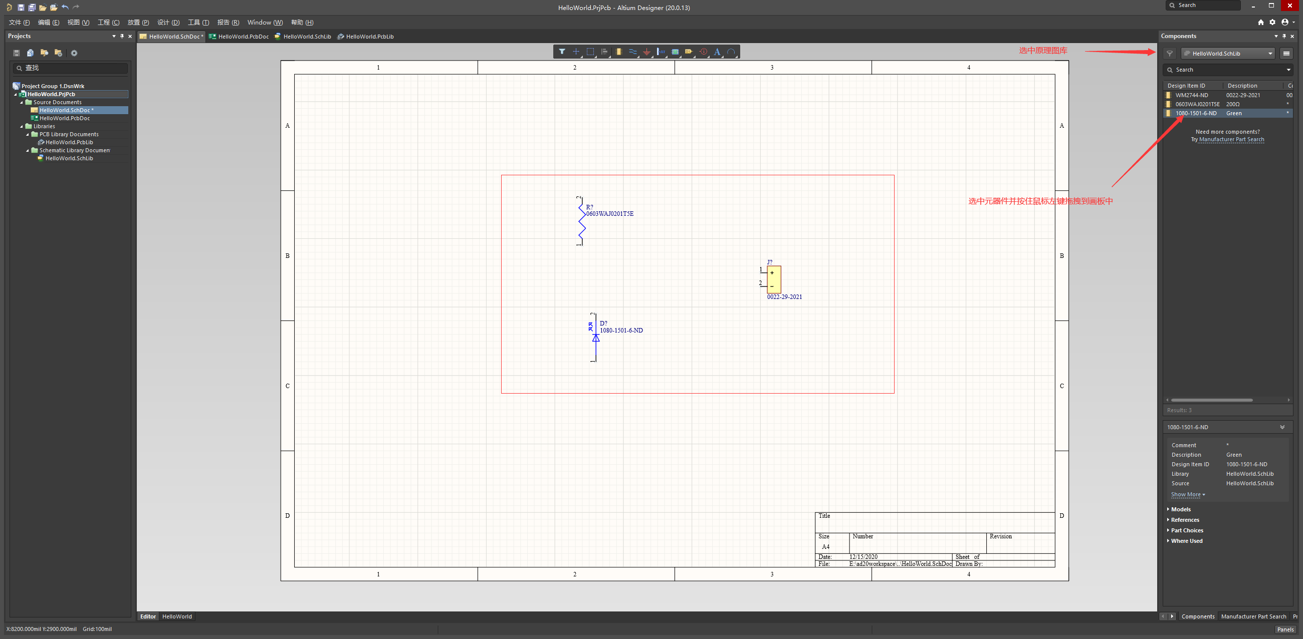
(1) Click the menu bar "Place" --->Line Harness->Line Harness Connector option or press the shortcut key <P>+<H>+<C>, and the cursor becomes a cross shape and has a harness connector shape.
(2) Move the cursor to the place you want to place, determine the starting point, and drag the mouse to determine the end point.
(3) Set the properties of the connector. During the process of placing the connector, the user can set the bus properties by himself. The Properties interface pops up by double-clicking the harness connector or placing the connector status at the cursor.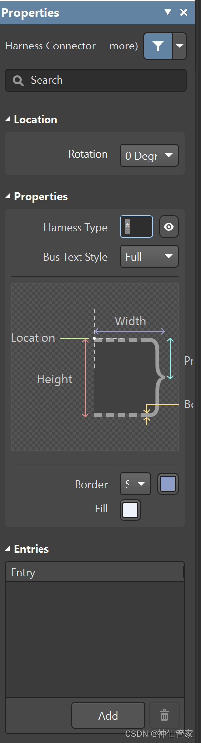
1.2 Wire Harness Entrance
The harness identifies each network or bus by the name of the harness entrance. Unless the harness connector is named, network naming generally does not use the name of the harness entrance.
(1) Click the menu bar "Place" --->Line Harness->Line Harness Entrance option or press the shortcut key <P>+<H>+<E>, and the cursor becomes a cross shape and has a harness connector shape.
(2) Move the cursor to the inside of the harness connector, click the left mouse button to select the position to be placed, and only the left border of the harness connector can be moved.
(3) Set the properties of the wiring harness entrance. During the process of placing the connector, the user can set the harness entry properties by himself. When double-click the harness entrance or place the harness entrance status at the cursor, press <Tab> to pop up the "Properties" interface.
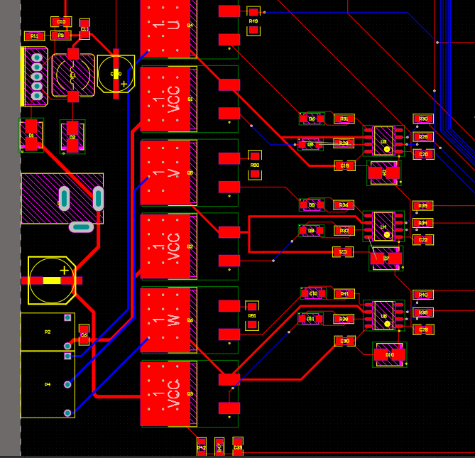
1.3 Signal wiring harness
A signal harness is a combination of a set of parallel signal lines of the same properties, connected to another wire connector on the same circuit diagram through the signal harness circuit, or connected to a circuit inlet or port to connect the signal to another schematic diagram.
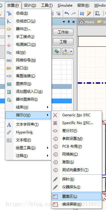
(1) Click the menu bar "Place" --->Line Harness->Signal Harness Option or press the shortcut key <P>+<H>+<H> At this time, the cursor becomes a cross shape and has a harness connector shape.
(2) Move the cursor to the pin of the component where you want to place the signal wiring harness and click the starting point of the signal wiring harness. A red symbol appears, indicating that the signal harness is placed successfully.
(3) Set the properties of the signal harness. During the process of placing the signal wiring harness, the user can set the signal wiring harness properties by himself. When double-clicking the signal harness or placing the signal harness at the cursor, press <Tab> to pop up the "Properties" interface.
Intelligent Recommendation
Basic knowledge of getting started with Altium Designer 20 (1)
Note: The following descriptions are based on the Altium Designer 20 (hereinafter referred to as: Ad 20) version Ad 20 basic terms Schematic gallery: by electronic devicesSchematic diagramIt forms a s...
Basic knowledge of getting started with Altium Designer 20 (4)
Content description, in the previous section we have completed the packaging of the components, the next section will describe how to bind the two libraries and how to draw the schematic diagram. Two ...
Getting started with Altium Designer-from schematic to printed circuit board
referenceOfficial website introductory tutorial。 If the above link fails or cannot be opened, the author still has a pdf version on the csdn,Please click here for reference。 Project Introduction The r...
Altium Designer(3)
In the PCB drawing process, after the layout of the components is completed, you can start wiring. You need to pay attention to a few points when wiring: 1. For larger current, use a wider line, gener...

Altium designer notes
Altium Designer usage Build project Open AD, a default will appearWorkspace, WorkSpace1.DsnWrk, we can save it to its own specified location, then rename it, for example rename it to MyWorkSpace.DsnWr...
More Recommendation
Altium Designer Notes 2
1, the compiler shield / Compile Mask Place-Directives-Compile Mask, this feature is not only available to certain regions do you want to ERC examination showed it, as long as it is possible to emulat...
Altium designer Operation notes
Altium designer operating notes table of Contents: 1, to find components 2, minimum spacing provided traces 3, check the pcb trace errors such as violation of the rules 4, the removal of select copper...
Altium Designer beginner notes
Altium Designer beginner's notes-send factory printing from scratch For beginners learning AD, this blog serves as a beginner's note for future review and sharing of learning experience. If there are ...
Altium Designer uses notes
Altium Designer uses notes...
Altium Designer circuit design 3
The schematic is very large. The drawing in the default state cannot meet the requirements (1) Change the size of the drawing Right click and then-Options-Document Options Modify the standard style an...