A common structure for medium to high resolution applications with sampling rates below 5Msps (million samples per second).
The resolution of SAR ADCs is generally from 8 bits to 16 bits, featuring low power consumption and small size.
These features make this type of ADC a wide range of applications, such as portable/battery-powered instruments, pen input quantizers, industrial control, and data/signal acquisition.
As the name suggests, SAR ADC essentially implements a binary search algorithm.
Therefore, when the internal circuit operates at several megahertz (MHz), the ADC sampling rate is only a fraction of this value due to the successive approximation algorithm.
SAR ADC architecture
Although the way to implement SAR ADCs varies widely, the basic structure is very simple (seefigure 1)。
The analog input voltage (VIN) is held by the sample/hold circuit.
To implement the binary search algorithm, the N-bit registers are first set to the middle scale (ie: 100...00, MSB is set to 1).
Thus, the DAC output (VDAC) is set to VREF/2, which is the reference voltage supplied to the ADC.
Then, the comparison judges whether VIN is smaller or larger than VDAC.
If VIN is greater than VDAC, the comparator outputs a logic high or 1 and the MSB of the N-bit register remains at 1.
Conversely, if VIN is less than VDAC, the comparator outputs a logic low and the MSB of the N-bit register is cleared.
The SAR control logic then moves to the next bit and sets this bit high for the next compare.
This process continues until the LSB. After the above operation is completed, the conversion is completed, and the N-bit conversion result is stored in the register.
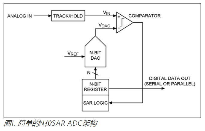
figure 2A 4-bit conversion example is given, and the y-axis (and the thick line in the figure) represents the output voltage of the DAC.
In this example, the first comparison shows VIN < VDAC. Therefore, bit 3 is set to zero.
The DAC is then set to 0100 and a second comparison is performed. Bit 2 remains at 1 due to VIN > VDAC.
The DAC is set to 0110 and a third comparison is performed. According to the comparison result, bit 1 is set to 0.
The DAC is again set to 0101 and the last comparison is performed.
Finally, bit 0 is determined to be 1 due to VIN > VDAC.
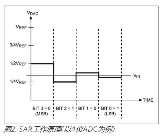
Note that four comparison cycles are required for a 4-bit ADC.
Typically, an N-bit SAR ADC requires N comparison cycles and must not enter the next conversion until the previous bit conversion is complete.
It can be seen that this type of ADC can effectively reduce power consumption and space. Of course, it is for this reason.
Successive approximation ADCs with resolutions ranging from 14 bits to 16 bits and rates above a few Msps (million samples per second) are extremely rare.
Another notable feature of SAR ADCs is that power consumption varies with sampling rate.
This is in contrast to flash ADCs or pipelined ADCs, which have fixed power consumption at different sampling rates.
This variable power consumption feature is advantageous for low power applications or applications that do not require continuous data acquisition (for example, for PDA digitizers).
In-depth analysis of SAR
Two important components of the SAR ADC are the comparator and the DAC, which we can see later.
The sample/hold circuit in Figure 1 can be embedded in the DAC, not as a separate circuit.
The speed of a SAR ADC is limited to:
- The setup time of the DAC must be stable within the resolution of the entire converter during this time (eg 1⁄2 LSB)
- The comparator must be able to resolve small differences between VIN and VDAC within the specified time.
- Logical overhead
DAC
The maximum settling time of a DAC is usually determined by the MSB setup time. The reason is simple. The MSB change represents the maximum offset of the DAC output.
In addition, the linearity of the ADC is also limited by the linearity of the DAC. Therefore, due to the inherent matching of components,
SAR ADCs with resolutions above 12 bits often require conditioning or calibration to improve their linearity.
Although this depends to some extent on the process and design, in actual DAC designs, component matching limits the linearity to around 12 bits.
Many SAR ADCs use capacitive DACs with inherent sample/hold functions.
Capacitive DACs generate analog output voltages based on the principle of charge redistribution. Since this type of DAC is very common in SAR ADCs, we'd better discuss how they work.
A capacitive DAC includes an array of N binary weighted capacitors and an "empty LSB" capacitor.
image 3It is an example of a 16-bit capacitive DAC connected to a comparator. During the sampling phase, the common end of the array (common point for all capacitor connections, see Figure 3) is grounded.
All free ends are connected to the input signal (analog input or VIN). After sampling, the common terminal is disconnected from the ground, and the free terminal is disconnected from VIN, effectively obtaining a charge amount proportional to the input voltage on the capacitor array.
Then, ground the free ends of all capacitors and drive the common to a negative voltage -VIN.
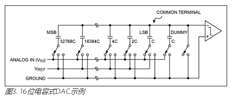
As a first step in the binary search algorithm, the bottom of the MSB capacitor is disconnected from ground and connected to VREF, driving the common-side voltage to 1⁄2VREF toward the positive terminal.
Therefore, VCOMMON = -VIN + 1⁄2 × VREF
If VCOMMON < 0 (ie VIN > 1⁄2 × VREF), the comparator output is a logic 1. If VIN < 1⁄2 × VREF, the comparator output is a logic '0'.
If the comparator output is a logic 1, the bottom of the MSB capacitor remains connected to VREF. Otherwise, the bottom of the MSB capacitor is connected to ground.
Next, the bottom of the next smaller capacitor is connected to VREF, which compares the new VCOMMON voltage to ground.
Continue the above process until the values of all the bits are determined.
In short, VCOMMON = -VIN + BN-1 × VREF/2 + BN-2 × VREF/4 + BN-1 × VREF/8 + ... + B0 × VREF/2N-1 (B_ is the comparator Output / ADC output bit).
Comparators
The comparator needs to have sufficient speed and accuracy, although the comparator's offset voltage does not affect the overall linearity.
It introduces a bias to the system's transmission characteristic curve and introduces an offset cancellation technique to reduce the comparator's offset voltage.
However, noise must also be considered, and the equivalent input noise of the comparator is typically designed to be within 1 LSB.
The comparator must be able to resolve the voltage within the accuracy of the entire system, which means that the comparator needs to be as accurate as the system.
Comparison of SAR ADC and other ADC structures
Compared to pipelined ADC
The pipelined ADC uses a parallel architecture in which each stage of the parallel structure is sampled one or more bits at a time.
This inherent parallelism increases data throughput, but at the expense of power consumption and latency.
The so-called delay, in this case, is defined as the time difference between the time the ADC samples the analog input and the time the quantized data is obtained at the output.
For example, a 5-stage pipelined ADC has at least 5 clock cycles of delay, while a SAR has only 1 clock cycle delay.
It should be noted that the definition of delay is only relative to the throughput of the ADC, not the internal clock of the SAR, which is many times the throughput.
Pipeline ADCs require frequent digital error calibration to reduce the accuracy requirements of each stage of the flash ADC (ie, comparator) on the pipeline.
The comparator accuracy of the SAR ADC only needs to be comparable to the accuracy of the overall system.
Pipelined ADCs typically require more silicon area than equivalent SARs.
As with SAR, pipelined ADCs with more than 12 bits of precision usually require some form of fine-tuning or calibration.
Compared to a flash ADC
The flash ADC consists of a large number of comparators, each of which includes a wideband, low gain preamplifier and latch.
The preamplifier must be used only to provide gain, does not require high linearity and high accuracy, which means that only the comparator threshold needs to have higher accuracy.
Therefore, the flash ADC is the fastest architecture at the current conversion rate.
It is often necessary to compromise on the speed of the flash ADC and the low power and small size characteristics of the SAR DAC.
Although extremely high speed 8-bit flash ADCs (and their fold/interpolation variants) have sample rates up to 1.5Gsps, it is difficult to find a 10-bit flash ADC.
The 12-bit (and higher) flash ADCs are not yet commercially available.
This is because for every 1 bit increase in resolution, the number of comparators in a flash ADC will multiply, while ensuring that the accuracy of the comparator is twice the accuracy of the system.
In SAR ADCs, increasing resolution requires more accurate components, but the complexity does not increase exponentially.
Of course, the speed of a SAR ADC cannot be compared to a flash ADC.
Compared to Σ-Δ converter
Traditional oversampling/Σ-Δ converters are commonly used in digital audio applications with bandwidth limitations of approximately 22 kHz.
Recently, some wideband sigma-delta converters have been able to achieve bandwidths from 1 MHz to 2 MHz with resolutions ranging from 12 bits to 16 bits.
This is typically done by a high order sigma-delta modulator (eg, 4th order or higher) with a multi-bit ADC and a multi-bit feedback DAC.
The sigma-delta converter has an inherent advantage over SAR ADCs:
That is, no special fine-tuning or calibration is required, even if the resolution reaches 16 to 18 bits.
Since the sampling rate of this type of ADC is much higher than the effective bandwidth, there is no need for an anti-aliasing filter that adds a fast roll-off at the analog input.
Processed by the back end digital filter. The oversampling characteristics of the sigma-delta converter can also be used to "smooth" any system noise in the analog input.
The sigma-delta converter is to exchange the resolution for the rate. Since generating a final sample requires sampling many times (at least 16 times, generally more),
This requires the internal analog circuit of the sigma-delta modulator to operate at a much faster rate than the final data rate.
The design of the digital decimation filter is also a challenge and consumes a considerable amount of silicon area.
In the near future, the bandwidth of the highest-speed, high-resolution sigma-delta converter will be less likely to be much higher than a few megahertz.
to sum up
In summary, the main advantages of SAR ADCs are low power consumption, high resolution, high precision, and small size.
Because of these advantages, SAR ADCs are often integrated with other larger functions.
The main limitation of the SAR architecture is the low sampling rate, and the various units (such as DACs and comparators) need to achieve comparable accuracy to the overall system.
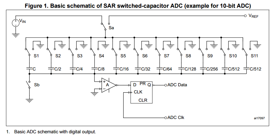
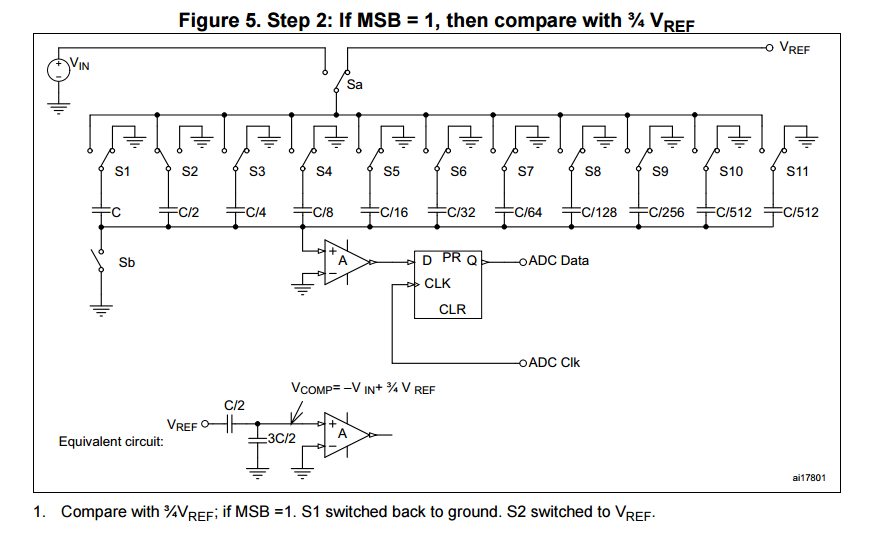
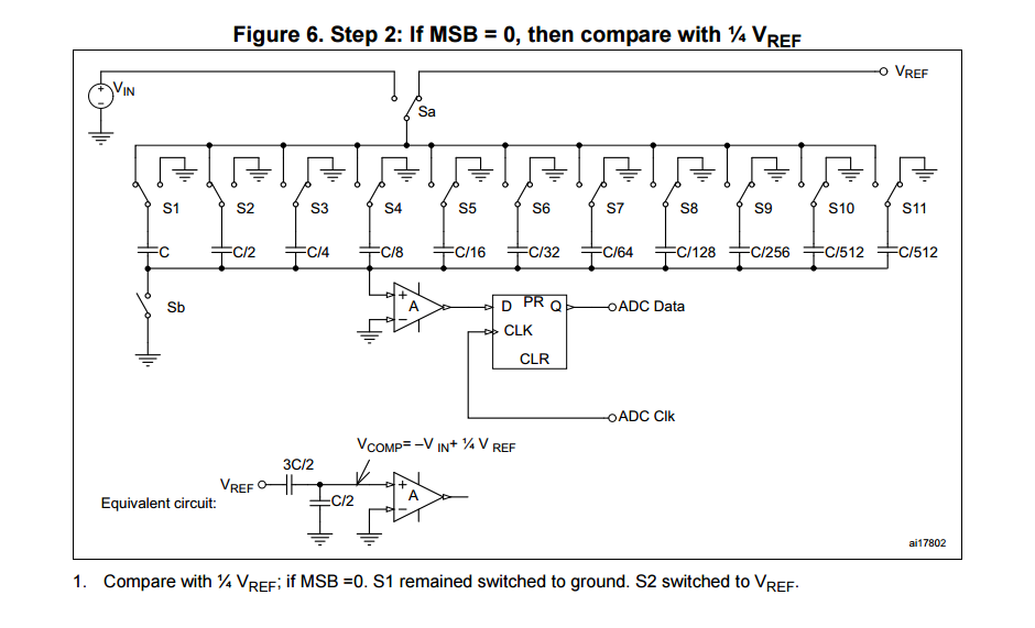
The ADC in STM32x microcontrollers uses the SAR (successive approximation register) principle,
by which the conversion is performed in several steps.
The number of conversion steps is equal to the number of bits in the ADC converter.
Each step is driven by the ADC clock.
Each ADC clock produces one bit from result to output.
ADC internal design is a switched-capacitor type.
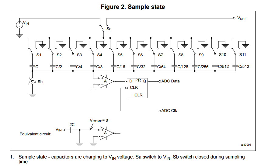
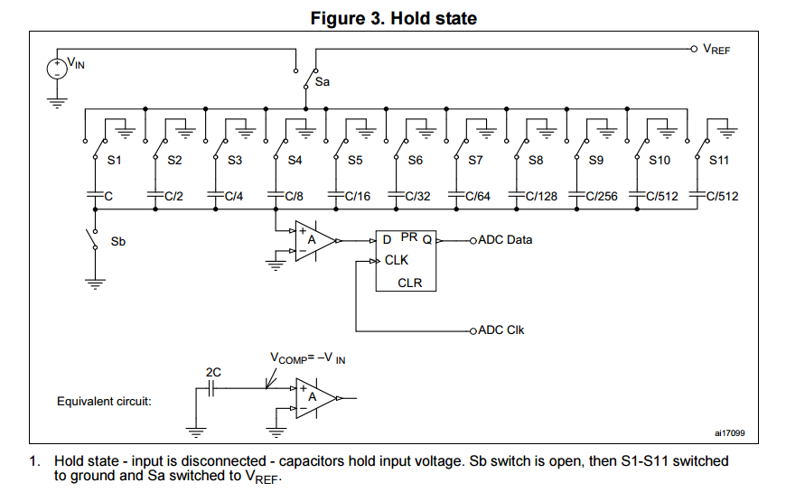
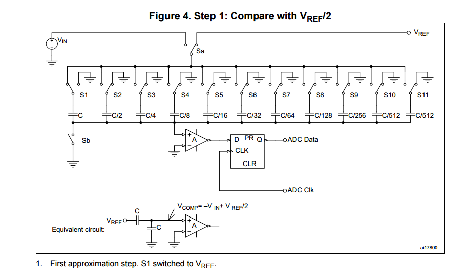
The following figures (Figure 1 to Figure 6) explain the principle of ADC operation.
The example given below shows only the first steps of approximation
but the process continues till the LSB is reached.